
Advanced Semiconductor Packaging Market
Advanced Semiconductor Packaging Market Forecasts to 2034 - Global Analysis By Packaging Type (Flip Chip Packaging, Wafer-Level Packaging, Fan-Out Packaging, 2.5D Interposer-Based Packaging, 3D IC Packaging, System-in-Package (SiP), Embedded Die Packaging, and Chiplet-Based Modular Packaging), Material, Process, Interconnection Technology, End User, and By Geography

|
Years Covered |
2023-2034 |
|
Estimated Year Value (2026) |
US $57.9 BN |
|
Projected Year Value (2032) |
US $123.3 BN |
|
CAGR (2026-2032) |
9.9% |
|
Regions Covered |
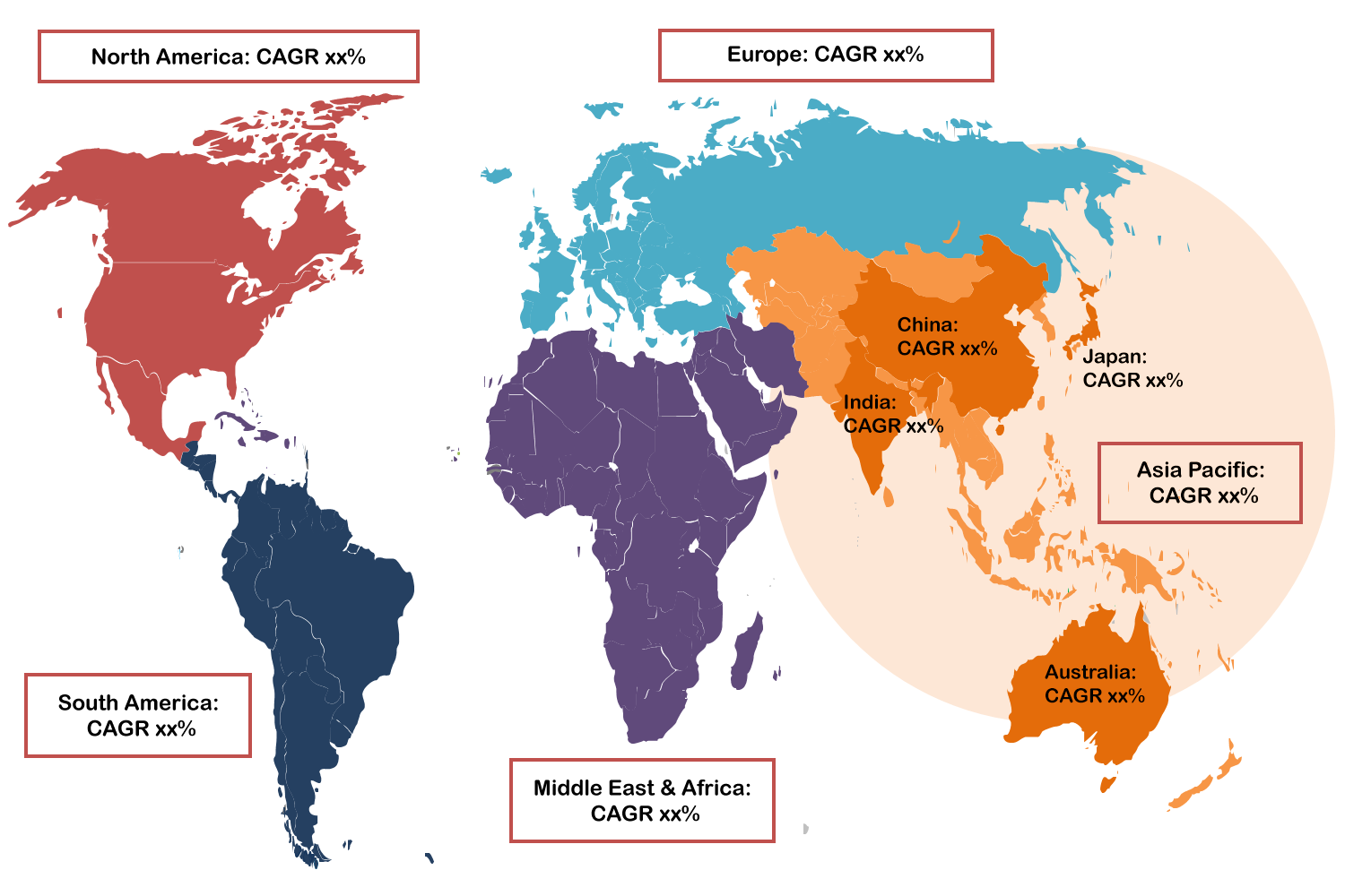
North America, Europe, Asia Pacific, South America, and Middle East & Africa |
|
Countries Covered |
US, Canada, Mexico, Germany, UK, Italy, France, Spain, Japan, China, India, Australia, New Zealand, South Korea, Rest of Asia Pacific, South America, Argentina, Brazil, Chile, Middle East & Africa, Saudi Arabia, UAE, Qatar, and South Africa |
|
Largest Market |
Asia Pacific |
|
Highest Growing Market |
Asia Pacific |
According to Stratistics MRC, the Global Advanced Semiconductor Packaging Market is accounted for $57.9 billion in 2026 and is expected to reach $123.3 billion by 2034 growing at a CAGR of 9.9% during the forecast period. The advanced semiconductor packaging market covers technologies that integrate multiple chips into compact, high-performance packages using methods such as 2.5D, 3D stacking, fan-out, and system-in-package architectures. It supports smartphones, data centers, automotive electronics, and AI hardware. Growth is driven by demand for higher computing performance, miniaturization, power efficiency improvements, slowing transistor scaling, and rising investments in heterogeneous integration and high-bandwidth memory solutions.
According to the SEMI, advanced packaging already represents over 45% of total semiconductor packaging revenue, driven by high-performance computing and AI chips.
Market Dynamics:
Driver:
Demand for higher performance and miniaturization in electronics
As smartphones, wearables, and high-performance computing (HPC) devices require greater functional density within shrinking footprints, traditional packaging reaches its physical limits. Advanced packaging addresses this by enabling the integration of multiple dies into a single, compact form factor. This transition significantly enhances signal speed, reduces power consumption, and improves thermal management. Consequently, the industry’s shift toward nanoscale components and high-density interconnects remains a fundamental force driving the adoption of sophisticated 2.5D and 3D integration technologies.
Restraint:
High technical complexity and capital cost
Establishing state-of-the-art facilities requires high-end lithography equipment and cleanroom environments comparable to front-end wafer fabrication, often costing hundreds of millions of dollars. Furthermore, managing the intricacies of interconnects density, thermal dissipation, and yield at sub-5nm nodes introduces steep learning curves for manufacturers. These escalating capital requirements and the technical risks associated with hybrid bonding and through-silicon via (TSV) processes can deter smaller players, potentially leading to market consolidation among a few well-capitalized industry leaders.
Opportunity:
Growth of chiplet-based designs and heterogeneous integration
The emergence of chiplet architectures presents a transformative opportunity by moving away from monolithic chip designs. By disaggregating complex systems into smaller functional blocks, manufacturers can optimize each component using the most cost-effective process node before integrating them via advanced packaging. This approach significantly boosts manufacturing yields and reduces overall development timelines. Heterogeneous integration allows for the seamless combining of diverse technologies such as logic, memory, and RF components into a single system. As Moore’s Law slows, these modular designs provide a scalable path to achieve the performance gains required for next-generation AI and 5G applications.
Threat:
Geopolitical tensions affecting supply chains
A vast majority of the world’s back-end assembly and testing capacity is concentrated in East Asia, any regional conflict or export control can lead to catastrophic supply chain disruptions. Recent trade barriers targeting critical AI chip technologies and specialized packaging tools have forced companies to rethink their geographic footprints. The race for "technological sovereignty" is leading to fragmented markets and increased operational costs as nations rush to reshore advanced manufacturing capabilities to mitigate vulnerability to foreign policy shifts.
Covid-19 Impact:
The COVID-19 pandemic initially hindered the market through widespread facility shutdowns and severe logistical bottlenecks that delayed the delivery of raw materials and equipment. However, the crisis also accelerated a surge in digital transformation, driving unprecedented demand for laptops, data centers, and healthcare electronics. This shift forced packaging providers to adopt AI-driven supply chain modeling and more resilient manufacturing strategies. While short-term labor shortages and component scarcity impacted production, the long-term effect has been an accelerated investment in advanced, automated packaging solutions to support a permanent increase in global digital consumption.
The flip chip packaging segment is expected to be the largest during the forecast period
The flip chip packaging segment is expected to account for the largest market share during the forecast period due to its superior electrical performance and proven reliability. By replacing traditional wire bonding with direct solder bump connections, flip chip technology facilitates higher I/O density and enhanced signal integrity, which are critical for high-speed processing. Its widespread adoption across consumer electronics, networking, and data centers ensures its continued dominance. Furthermore, advancements such as copper pillar technology and fine-pitch micro-bumping have extended the life of this segment.
The automotive electronics segment is expected to have the highest CAGR during the forecast period
Over the forecast period, the automotive electronics segment is predicted to witness the highest growth rate as vehicles evolve into sophisticated mobile computing platforms. The rapid shift toward Electric Vehicles (EVs) and Autonomous Driving (AD) systems necessitates advanced semiconductor solutions that can operate reliably in harsh environments. Advanced packaging is essential for integrating the complex sensors, AI accelerators, and power management ICs required for modern safety and infotainment features. As automotive manufacturers prioritize energy efficiency and compact system designs, the demand for specialized, high-reliability packaging technologies is projected to outpace growth in traditional consumer electronics sectors.
Region with largest share:
During the forecast period, the Asia Pacific region is expected to hold the largest market share, anchored by a robust ecosystem of foundries and Outsourced Semiconductor Assembly and Test (OSAT) providers. Countries such as Taiwan, China, and South Korea serve as the global hubs for semiconductor manufacturing, supported by massive government subsidies and infrastructure investments. The presence of major industry players like TSMC, Samsung, and JCET allows the region to leverage economies of scale and technical expertise. Additionally, the proximity to a massive consumer electronics manufacturing base further solidifies Asia Pacific’s position as the primary engine for advanced packaging production.
Region with highest CAGR:
Over the forecast period, the Asia Pacific region is anticipated to exhibit the highest CAGR as it continues to attract significant investments in next-generation packaging facilities. While it already leads in volume, the region is rapidly transitioning toward high-end technologies like 2.5D and 3D stacking to support the booming AI and 5G markets. Strategic initiatives, such as China’s domestic self-sufficiency programs and Japan’s efforts to revitalize its semiconductor sector through advanced packaging, are driving rapid expansion.
Key players in the market
Some of the key players in Advanced Semiconductor Packaging Market include Taiwan Semiconductor Manufacturing Company Limited, Intel Corporation, Samsung Electronics Co., Ltd., ASE Technology Holding Co., Ltd., Amkor Technology, Inc., Siliconware Precision Industries Co., Ltd., JCET Group Co., Ltd., Powertech Technology Inc., STATS ChipPAC, ChipMOS Technologies Inc., Broadcom Inc., Texas Instruments Incorporated, NXP Semiconductors N.V., Micron Technology, Inc., and United Microelectronics Corporation.
Key Developments:
In February 2026, TSMC announced it is increasing its CoWoS (Chip on Wafer on Substrate) monthly capacity forecast to 127,000 wafers by the end of 2026 to meet surging demand for AI accelerators and high-end GPUs.
In October 2025, Bloomberg Intelligence reported that TSMC, ASE, and Amkor are positioned to dominate 2.5D and 3D packaging, with market growth projected at 26% annually.
Packaging Types Covered:
• Flip Chip Packaging
• Wafer-Level Packaging
• Fan-Out Packaging
• 2.5D Interposer-Based Packaging
• 3D IC Packaging
• System-in-Package (SiP)
• Embedded Die Packaging
• Chiplet-Based Modular Packaging
Materials Covered:
• Substrates
• Interposers
• Die Attach Materials
• Encapsulation and Mold Compounds
• Underfill Materials
• Thermal Interface Materials
• Solder and Conductive Materials
Processes Covered:
• Front-End Packaging Processes
• Wafer Bumping and Redistribution
• Die Attach and Placement
• Bonding and Interconnection
• Encapsulation and Molding
• Singulation and Final Assembly
• Testing and Inspection
Interconnection Technologies Covered:
• Wire Bonding (Advanced Variants)
• Micro-Bump Interconnects
• Copper Pillar Bumps
• Hybrid Bonding
• Through-Silicon Via (TSV)
• Redistribution Layer (RDL)
End Users Covered:
• Consumer Electronics
• Data Centers and Cloud Computing
• Telecommunications and Networking
• Automotive Electronics
• Industrial Automation and Robotics
• Healthcare and Medical Devices
• Aerospace and Defense
• Energy and Power Electronics
Regions Covered:
• North America
o United States
o Canada
o Mexico
• Europe
o United Kingdom
o Germany
o France
o Italy
o Spain
o Netherlands
o Belgium
o Sweden
o Switzerland
o Poland
o Rest of Europe
• Asia Pacific
o China
o Japan
o India
o South Korea
o Australia
o Indonesia
o Thailand
o Malaysia
o Singapore
o Vietnam
o Rest of Asia Pacific
• South America
o Brazil
o Argentina
o Colombia
o Chile
o Peru
o Rest of South America
• Rest of the World (RoW)
o Middle East
§ Saudi Arabia
§ United Arab Emirates
§ Qatar
§ Israel
§ Rest of Middle East
o Africa
§ South Africa
§ Egypt
§ Morocco
§ Rest of Africa
What our report offers:
- Market share assessments for the regional and country-level segments
- Strategic recommendations for the new entrants
- Covers Market data for the years 2023, 2024, 2025, 2026, 2027, 2028, 2030, 2032 and 2034
- Market Trends (Drivers, Constraints, Opportunities, Threats, Challenges, Investment Opportunities, and recommendations)
- Strategic recommendations in key business segments based on the market estimations
- Competitive landscaping mapping the key common trends
- Company profiling with detailed strategies, financials, and recent developments
- Supply chain trends mapping the latest technological advancements
Free Customization Offerings:
All the customers of this report will be entitled to receive one of the following free customization options:
• Company Profiling
o Comprehensive profiling of additional market players (up to 3)
o SWOT Analysis of key players (up to 3)
• Regional Segmentation
o Market estimations, Forecasts and CAGR of any prominent country as per the client's interest (Note: Depends on feasibility check)
• Competitive Benchmarking
o Benchmarking of key players based on product portfolio, geographical presence, and strategic alliances
Table of Contents
1 Executive Summary
1.1 Market Snapshot and Key Highlights
1.2 Growth Drivers, Challenges, and Opportunities
1.3 Competitive Landscape Overview
1.4 Strategic Insights and Recommendations
2 Research Framework
2.1 Study Objectives and Scope
2.2 Stakeholder Analysis
2.3 Research Assumptions and Limitations
2.4 Research Methodology
2.4.1 Data Collection (Primary and Secondary)
2.4.2 Data Modeling and Estimation Techniques
2.4.3 Data Validation and Triangulation
2.4.4 Analytical and Forecasting Approach
3 Market Dynamics and Trend Analysis
3.1 Market Definition and Structure
3.2 Key Market Drivers
3.3 Market Restraints and Challenges
3.4 Growth Opportunities and Investment Hotspots
3.5 Industry Threats and Risk Assessment
3.6 Technology and Innovation Landscape
3.7 Emerging and High-Growth Markets
3.8 Regulatory and Policy Environment
3.9 Impact of COVID-19 and Recovery Outlook
4 Competitive and Strategic Assessment
4.1 Porter's Five Forces Analysis
4.1.1 Supplier Bargaining Power
4.1.2 Buyer Bargaining Power
4.1.3 Threat of Substitutes
4.1.4 Threat of New Entrants
4.1.5 Competitive Rivalry
4.2 Market Share Analysis of Key Players
4.3 Product Benchmarking and Performance Comparison
5 Global Advanced Semiconductor Packaging Market, By Packaging Type
5.1 Flip Chip Packaging
5.2 Wafer-Level Packaging
5.3 Fan-Out Packaging
5.4 2.5D Interposer-Based Packaging
5.5 3D IC Packaging
5.6 System-in-Package (SiP)
5.7 Embedded Die Packaging
5.8 Chiplet-Based Modular Packaging
6 Global Advanced Semiconductor Packaging Market, By Material
6.1 Substrates
6.1.1 Organic Substrates
6.1.2 Ceramic Substrates
6.1.3 Glass Substrates
6.2 Interposers
6.2.1 Silicon
6.2.2 Organic
6.2.3 Glass
6.3 Die Attach Materials
6.4 Encapsulation and Mold Compounds
6.5 Underfill Materials
6.6 Thermal Interface Materials
6.7 Solder and Conductive Materials
7 Global Advanced Semiconductor Packaging Market, By Process
7.1 Front-End Packaging Processes
7.2 Wafer Bumping and Redistribution
7.3 Die Attach and Placement
7.4 Bonding and Interconnection
7.5 Encapsulation and Molding
7.6 Singulation and Final Assembly
7.7 Testing and Inspection
8 Global Advanced Semiconductor Packaging Market, By Interconnection Technology
8.1 Wire Bonding (Advanced Variants)
8.2 Micro-Bump Interconnects
8.3 Copper Pillar Bumps
8.4 Hybrid Bonding
8.5 Through-Silicon Via (TSV)
8.6 Redistribution Layer (RDL)
9 Global Advanced Semiconductor Packaging Market, By End User
9.1 Consumer Electronics
9.2 Data Centers and Cloud Computing
9.3 Telecommunications and Networking
9.4 Automotive Electronics
9.5 Industrial Automation and Robotics
9.6 Healthcare and Medical Devices
9.7 Aerospace and Defense
9.8 Energy and Power Electronics
10 Global Advanced Semiconductor Packaging Market, By Geography
10.1 North America
10.1.1 United States
10.1.2 Canada
10.1.3 Mexico
10.2 Europe
10.2.1 United Kingdom
10.2.2 Germany
10.2.3 France
10.2.4 Italy
10.2.5 Spain
10.2.6 Netherlands
10.2.7 Belgium
10.2.8 Sweden
10.2.9 Switzerland
10.2.10 Poland
10.2.11 Rest of Europe
10.3 Asia Pacific
10.3.1 China
10.3.2 Japan
10.3.3 India
10.3.4 South Korea
10.3.5 Australia
10.3.6 Indonesia
10.3.7 Thailand
10.3.8 Malaysia
10.3.9 Singapore
10.3.10 Vietnam
10.3.11 Rest of Asia Pacific
10.4 South America
10.4.1 Brazil
10.4.2 Argentina
10.4.3 Colombia
10.4.4 Chile
10.4.5 Peru
10.4.6 Rest of South America
10.5 Rest of the World (RoW)
10.5.1 Middle East
10.5.1.1 Saudi Arabia
10.5.1.2 United Arab Emirates
10.5.1.3 Qatar
10.5.1.4 Israel
10.5.1.5 Rest of Middle East
10.5.2 Africa
10.5.2.1 South Africa
10.5.2.2 Egypt
10.5.2.3 Morocco
10.5.2.4 Rest of Africa
11 Strategic Market Intelligence
11.1 Industry Value Network and Supply Chain Assessment
11.2 White-Space and Opportunity Mapping
11.3 Product Evolution and Market Life Cycle Analysis
11.4 Channel, Distributor, and Go-to-Market Assessment
12 Industry Developments and Strategic Initiatives
12.1 Mergers and Acquisitions
12.2 Partnerships, Alliances, and Joint Ventures
12.3 New Product Launches and Certifications
12.4 Capacity Expansion and Investments
12.5 Other Strategic Initiatives
13 Company Profiles
13.1 Taiwan Semiconductor Manufacturing Company Limited
13.2 Intel Corporation
13.3 Samsung Electronics Co., Ltd.
13.4 ASE Technology Holding Co., Ltd.
13.5 Amkor Technology, Inc.
13.6 Siliconware Precision Industries Co., Ltd.
13.7 JCET Group Co., Ltd.
13.8 Powertech Technology Inc.
13.9 STATS ChipPAC
13.10 ChipMOS Technologies Inc.
13.11 Broadcom Inc.
13.12 Texas Instruments Incorporated
13.13 NXP Semiconductors N.V.
13.14 Micron Technology, Inc.
13.15 United Microelectronics Corporation
List of Tables
1 Global Advanced Semiconductor Packaging Market Outlook, By Region (2023–2034) ($MN)
2 Global Advanced Semiconductor Packaging Market Outlook, By Packaging Type (2023–2034) ($MN)
3 Global Advanced Semiconductor Packaging Market Outlook, By Flip Chip Packaging (2023–2034) ($MN)
4 Global Advanced Semiconductor Packaging Market Outlook, By Wafer-Level Packaging (2023–2034) ($MN)
5 Global Advanced Semiconductor Packaging Market Outlook, By Fan-Out Packaging (2023–2034) ($MN)
6 Global Advanced Semiconductor Packaging Market Outlook, By 2.5D Interposer-Based Packaging (2023–2034) ($MN)
7 Global Advanced Semiconductor Packaging Market Outlook, By 3D IC Packaging (2023–2034) ($MN)
8 Global Advanced Semiconductor Packaging Market Outlook, By System-in-Package (SiP) (2023–2034) ($MN)
9 Global Advanced Semiconductor Packaging Market Outlook, By Embedded Die Packaging (2023–2034) ($MN)
10 Global Advanced Semiconductor Packaging Market Outlook, By Chiplet-Based Modular Packaging (2023–2034) ($MN)
11 Global Advanced Semiconductor Packaging Market Outlook, By Material (2023–2034) ($MN)
12 Global Advanced Semiconductor Packaging Market Outlook, By Substrates (2023–2034) ($MN)
13 Global Advanced Semiconductor Packaging Market Outlook, By Organic Substrates (2023–2034) ($MN)
14 Global Advanced Semiconductor Packaging Market Outlook, By Ceramic Substrates (2023–2034) ($MN)
15 Global Advanced Semiconductor Packaging Market Outlook, By Glass Substrates (2023–2034) ($MN)
16 Global Advanced Semiconductor Packaging Market Outlook, By Interposers (2023–2034) ($MN)
17 Global Advanced Semiconductor Packaging Market Outlook, By Silicon Interposers (2023–2034) ($MN)
18 Global Advanced Semiconductor Packaging Market Outlook, By Organic Interposers (2023–2034) ($MN)
19 Global Advanced Semiconductor Packaging Market Outlook, By Glass Interposers (2023–2034) ($MN)
20 Global Advanced Semiconductor Packaging Market Outlook, By Die Attach Materials (2023–2034) ($MN)
21 Global Advanced Semiconductor Packaging Market Outlook, By Encapsulation and Mold Compounds (2023–2034) ($MN)
22 Global Advanced Semiconductor Packaging Market Outlook, By Underfill Materials (2023–2034) ($MN)
23 Global Advanced Semiconductor Packaging Market Outlook, By Thermal Interface Materials (2023–2034) ($MN)
24 Global Advanced Semiconductor Packaging Market Outlook, By Solder and Conductive Materials (2023–2034) ($MN)
25 Global Advanced Semiconductor Packaging Market Outlook, By Process (2023–2034) ($MN)
26 Global Advanced Semiconductor Packaging Market Outlook, By Front-End Packaging Processes (2023–2034) ($MN)
27 Global Advanced Semiconductor Packaging Market Outlook, By Wafer Bumping and Redistribution (2023–2034) ($MN)
28 Global Advanced Semiconductor Packaging Market Outlook, By Die Attach and Placement (2023–2034) ($MN)
29 Global Advanced Semiconductor Packaging Market Outlook, By Bonding and Interconnection (2023–2034) ($MN)
30 Global Advanced Semiconductor Packaging Market Outlook, By Encapsulation and Molding (2023–2034) ($MN)
31 Global Advanced Semiconductor Packaging Market Outlook, By Singulation and Final Assembly (2023–2034) ($MN)
32 Global Advanced Semiconductor Packaging Market Outlook, By Testing and Inspection (2023–2034) ($MN)
33 Global Advanced Semiconductor Packaging Market Outlook, By Interconnection Technology (2023–2034) ($MN)
34 Global Advanced Semiconductor Packaging Market Outlook, By Wire Bonding (Advanced Variants) (2023–2034) ($MN)
35 Global Advanced Semiconductor Packaging Market Outlook, By Micro-Bump Interconnects (2023–2034) ($MN)
36 Global Advanced Semiconductor Packaging Market Outlook, By Copper Pillar Bumps (2023–2034) ($MN)
37 Global Advanced Semiconductor Packaging Market Outlook, By Hybrid Bonding (2023–2034) ($MN)
38 Global Advanced Semiconductor Packaging Market Outlook, By Through-Silicon Via (TSV) (2023–2034) ($MN)
39 Global Advanced Semiconductor Packaging Market Outlook, By Redistribution Layer (RDL) (2023–2034) ($MN)
40 Global Advanced Semiconductor Packaging Market Outlook, By End User (2023–2034) ($MN)
41 Global Advanced Semiconductor Packaging Market Outlook, By Consumer Electronics (2023–2034) ($MN)
42 Global Advanced Semiconductor Packaging Market Outlook, By Data Centers and Cloud Computing (2023–2034) ($MN)
43 Global Advanced Semiconductor Packaging Market Outlook, By Telecommunications and Networking (2023–2034) ($MN)
44 Global Advanced Semiconductor Packaging Market Outlook, By Automotive Electronics (2023–2034) ($MN)
45 Global Advanced Semiconductor Packaging Market Outlook, By Industrial Automation and Robotics (2023–2034) ($MN)
46 Global Advanced Semiconductor Packaging Market Outlook, By Healthcare and Medical Devices (2023–2034) ($MN)
47 Global Advanced Semiconductor Packaging Market Outlook, By Aerospace and Defense (2023–2034) ($MN)
48 Global Advanced Semiconductor Packaging Market Outlook, By Energy and Power Electronics (2023–2034) ($MN)
Note: Tables for North America, Europe, APAC, South America, and Rest of the World (RoW) Regions are also represented in the same manner as above.
List of Figures
RESEARCH METHODOLOGY
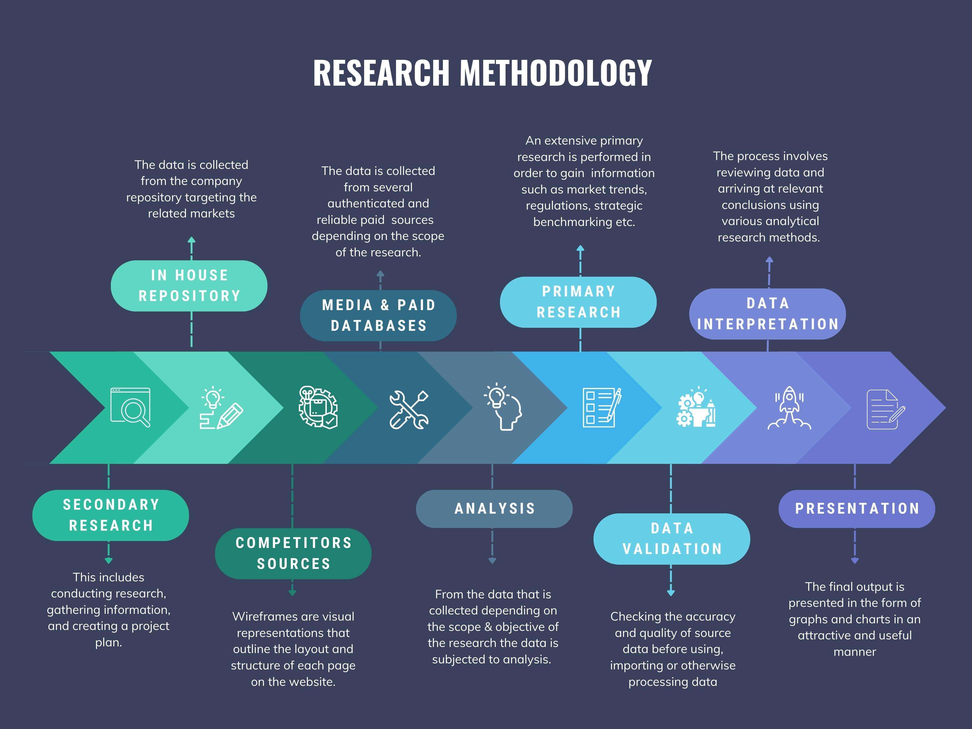
We at ‘Stratistics’ opt for an extensive research approach which involves data mining, data validation, and data analysis. The various research sources include in-house repository, secondary research, competitor’s sources, social media research, client internal data, and primary research.
Our team of analysts prefers the most reliable and authenticated data sources in order to perform the comprehensive literature search. With access to most of the authenticated data bases our team highly considers the best mix of information through various sources to obtain extensive and accurate analysis.
Each report takes an average time of a month and a team of 4 industry analysts. The time may vary depending on the scope and data availability of the desired market report. The various parameters used in the market assessment are standardized in order to enhance the data accuracy.
Data Mining
The data is collected from several authenticated, reliable, paid and unpaid sources and is filtered depending on the scope & objective of the research. Our reports repository acts as an added advantage in this procedure. Data gathering from the raw material suppliers, distributors and the manufacturers is performed on a regular basis, this helps in the comprehensive understanding of the products value chain. Apart from the above mentioned sources the data is also collected from the industry consultants to ensure the objective of the study is in the right direction.
Market trends such as technological advancements, regulatory affairs, market dynamics (Drivers, Restraints, Opportunities and Challenges) are obtained from scientific journals, market related national & international associations and organizations.
Data Analysis
From the data that is collected depending on the scope & objective of the research the data is subjected for the analysis. The critical steps that we follow for the data analysis include:
- Product Lifecycle Analysis
- Competitor analysis
- Risk analysis
- Porters Analysis
- PESTEL Analysis
- SWOT Analysis
The data engineering is performed by the core industry experts considering both the Marketing Mix Modeling and the Demand Forecasting. The marketing mix modeling makes use of multiple-regression techniques to predict the optimal mix of marketing variables. Regression factor is based on a number of variables and how they relate to an outcome such as sales or profits.
Data Validation
The data validation is performed by the exhaustive primary research from the expert interviews. This includes telephonic interviews, focus groups, face to face interviews, and questionnaires to validate our research from all aspects. The industry experts we approach come from the leading firms, involved in the supply chain ranging from the suppliers, distributors to the manufacturers and consumers so as to ensure an unbiased analysis.
We are in touch with more than 15,000 industry experts with the right mix of consultants, CEO's, presidents, vice presidents, managers, experts from both supply side and demand side, executives and so on.
The data validation involves the primary research from the industry experts belonging to:
- Leading Companies
- Suppliers & Distributors
- Manufacturers
- Consumers
- Industry/Strategic Consultants
Apart from the data validation the primary research also helps in performing the fill gap research, i.e. providing solutions for the unmet needs of the research which helps in enhancing the reports quality.
For more details about research methodology, kindly write to us at info@strategymrc.com
Frequently Asked Questions
In case of any queries regarding this report, you can contact the customer service by filing the “Inquiry Before Buy” form available on the right hand side. You may also contact us through email: info@strategymrc.com or phone: +1-301-202-5929
Yes, the samples are available for all the published reports. You can request them by filling the “Request Sample” option available in this page.
Yes, you can request a sample with your specific requirements. All the customized samples will be provided as per the requirement with the real data masked.
All our reports are available in Digital PDF format. In case if you require them in any other formats, such as PPT, Excel etc you can submit a request through “Inquiry Before Buy” form available on the right hand side. You may also contact us through email: info@strategymrc.com or phone: +1-301-202-5929
We offer a free 15% customization with every purchase. This requirement can be fulfilled for both pre and post sale. You may send your customization requirements through email at info@strategymrc.com or call us on +1-301-202-5929.
We have 3 different licensing options available in electronic format.
- Single User Licence: Allows one person, typically the buyer, to have access to the ordered product. The ordered product cannot be distributed to anyone else.
- 2-5 User Licence: Allows the ordered product to be shared among a maximum of 5 people within your organisation.
- Corporate License: Allows the product to be shared among all employees of your organisation regardless of their geographical location.
All our reports are typically be emailed to you as an attachment.
To order any available report you need to register on our website. The payment can be made either through CCAvenue or PayPal payments gateways which accept all international cards.
We extend our support to 6 months post sale. A post sale customization is also provided to cover your unmet needs in the report.
Request Customization
We offer complimentary customization of up to 15% with every purchase. To share your customization requirements, feel free to email us at info@strategymrc.com or call us on +1-301-202-5929. .
Please Note: Customization within the 15% threshold is entirely free of charge. If your request exceeds this limit, we will conduct a feasibility assessment. Following that, a detailed quote and timeline will be provided.
WHY CHOOSE US ?

Assured Quality
Best in class reports with high standard of research integrity

24X7 Research Support
Continuous support to ensure the best customer experience.

Free Customization
Adding more values to your product of interest.

Safe & Secure Access
Providing a secured environment for all online transactions.

Trusted by 600+ Brands
Serving the most reputed brands across the world.