
Ai Based Semiconductor Defect Detection Market
AI-Based Semiconductor Defect Detection Market Forecasts to 2034 – Global Analysis By Inspection Type (Wafer Inspection, Mask and Reticle Inspection, Semiconductor Packaging Inspection, Die Inspection and Other Inspection Types), Defect Type, Component, AI Technology, Application, End User and By Geography

Market Dynamics:
Driver:
Rising Complexity of Advanced Nodes
The accelerating complexity of advanced semiconductor manufacturing is a primary driver for AI-based defect detection, as transistor architectures at 2nm and below generate defect densities and stochastic variations that conventional rule-based inspection cannot reliably classify. High-NA EUV lithography and gate-all-around transistor structures introduce buried defects and process drift patterns that require continuous model retraining, while AI inspection systems enable fabs to process petabytes of wafer image data in real time. This complexity sustains demand for inspection platforms that combine high-throughput optics with deep learning classification, thereby supporting yield protection at leading-edge nodes.
Restraint:
High Integration and Deployment Costs
The substantial capital and operational costs associated with AI inspection deployment represent a structural restraint on market expansion, because effective systems require advanced imaging hardware, GPU computing infrastructure, model training data pipelines, and deep integration with fab process control software. Smaller foundries and OSAT providers face particular barriers to adoption, as the investment required for a full AI inspection stack may exceed the cost of several traditional inspection tools. These economics limit deployment to high-volume, leading-edge facilities, which in turn constrains the pace of market penetration across the broader semiconductor manufacturing base.
Opportunity:
Smart Fab and Predictive Yield Analytics
The emergence of smart fab initiatives and predictive process analytics presents a significant opportunity for AI defect detection providers, as manufacturers increasingly seek to connect inspection data with manufacturing execution systems, equipment health monitoring, and yield prediction models. AI inspection platforms can generate not only defect maps but also actionable process signals that inform lithography tuning, etch compensation, and maintenance scheduling, which expands the value proposition beyond pure detection. Vendors capable of delivering integrated manufacturing intelligence solutions can capture share in the growing market for fab-wide process control and yield optimization.
Threat:
Model Reliability Under Process Drift
Algorithm reliability under changing process conditions poses a persistent threat to AI inspection adoption, because deep learning models trained on historical wafer data can degrade in accuracy when process recipes are modified, new materials are introduced, or tool conditions shift. The need for continuous model retraining and validation creates operational overhead for fabs, while false positives and missed defects carry direct yield and cost consequences. If AI models cannot demonstrate consistent performance across process changes, manufacturers may limit their reliance on automated classification and retain manual review steps, which slows the shift toward fully autonomous inspection workflows.
Covid-19 Impact:
The pandemic initially disrupted semiconductor inspection deployment as fab construction timelines slipped and equipment installation was delayed by travel restrictions and supply chain constraints. Mid-pandemic, demand for inspection tools proved resilient because chip shortages pushed manufacturers to maximize yield and accelerate process control investments. Post-pandemic, the structural impact has been a sustained emphasis on supply chain resilience and regional fab expansion, which supports long-term demand for automated inspection solutions as new facilities in the United States, Europe, and India seek to establish yield ramps with limited experienced engineering staff.
The wafer inspection segment is expected to be the largest during the forecast period
The wafer inspection segment is expected to account for the largest market share during the forecast period, due to its position as the primary quality gate in front-end semiconductor manufacturing, where defect detection directly determines yield and reliability outcomes. Wafer inspection encompasses patterned and unpatterned wafer review across lithography, etch, and deposition steps, and it generates the largest volume of image data that AI models must process. While mask inspection and packaging inspection are essential, wafer-level detection carries the highest value per inspected unit, thereby anchoring its dominant revenue position across the forecast horizon.
The deep learning segment is expected to have the highest CAGR during the forecast period
Over the forecast period, the deep learning segment is predicted to witness the highest growth rate, driven by the superior performance of convolutional neural networks and vision transformers in classifying complex defect patterns that rule-based algorithms cannot distinguish. Leading inspection platforms are increasingly embedding deep learning models for automated defect review and nuisance suppression, as fabs seek to reduce manual review burden while maintaining classification accuracy. The expanding availability of labeled wafer image datasets and GPU computing capacity further supports model training and deployment, which in turn accelerates adoption of deep learning-based inspection across advanced logic, memory, and packaging applications.
Region with largest share:
During the forecast period, the Asia Pacific region is expected to hold the largest market share, due to its concentration of leading-edge foundry and memory manufacturing capacity in Taiwan, South Korea, Japan, and China. TSMC, Samsung, and SK Hynix operate the most advanced nodes and generate the highest volumes of inspection data requiring AI classification, while Japanese equipment vendors such as Lasertec and Hitachi High-Tech supply critical inspection platforms to these fabs. Government semiconductor investment programs in China and India further expand regional inspection demand, and the presence of KLA, Applied Materials, and Onto Innovation customer bases reinforces Asia Pacific’s dominant position in AI defect detection deployment.
Region with highest CAGR:
Over the forecast period, the North America region is anticipated to exhibit the highest CAGR, due to the rapid expansion of domestic semiconductor manufacturing under the CHIPS Act and the corresponding need for advanced process control at newly constructed fabs. Intel, Micron, and TSMC Arizona are establishing leading-edge capacity that requires AI inspection systems from the start of production, while the region’s concentration of AI algorithm development expertise supports local innovation in defect classification models. Government funding for semiconductor R&D and smart manufacturing initiatives further stimulates adoption, and these catalysts together position North America for the fastest growth trajectory in the AI-based defect detection market.
Key players in the market
Some of the key players in AI-Based Semiconductor Defect Detection Market include KLA Corporation, Applied Materials, Inc., ASML Holding N.V., Hitachi High-Tech Corporation, Onto Innovation Inc., Camtek Ltd., Lasertec Corporation, Nova Ltd., SCREEN Holdings Co., Ltd., Tokyo Electron Limited, PDF Solutions, Inc., Siemens AG, Cognex Corporation, ZEISS Group, Nikon Corporation, Advantest Corporation, Teradyne, Inc., and Koh Young Technology Inc.
Key Developments:
In September 2026, Hitachi High-Tech Corporation accelerated its joint development framework with ZEISS for next-generation multi-beam inspection tools, integrating 91-beam multi-column technology with AI-assisted inspection algorithms to achieve defect detection speeds several dozen times faster than single-beam systems for 2nm and High-NA EUV production.
In September 2026, KLA Corporation presented its AI-powered inspection architecture at SEMICON Taiwan, combining GPU, high-bandwidth memory, and physics-based algorithms with foundation models to detect latent defects in AI accelerator packages containing multiple compute dies and HBM stacks.
In August 2026, Applied Materials, Inc. advanced adoption of its SEMVision G9 defect review system, which integrates proprietary ADR and ADC AI engines for single-image detection and CAD-based defect classification, reducing manual review requirements while accelerating high-confidence production decisions across logic and memory fabs
Inspection Types Covered:
• Wafer Inspection
• Mask and Reticle Inspection
• Semiconductor Packaging Inspection
• Die Inspection
• Other Inspection Types
Defect Types Covered:
• Particle and Contamination Defects
• Pattern Defects
• Surface Defects
• Structural Defects
• Packaging and Interconnect Defects
• Other Defect Types
Components Covered:
• Hardware
• Software
• Services
AI Technologies Covered:
• Machine Learning
• Deep Learning
• Computer Vision
• Other AI Technologies
Applications Covered:
• Wafer Fabrication
• Photolithography
• Etching and Deposition
• Semiconductor Assembly and Packaging
• Final Testing and Quality Control
• Other Applications
End Users Covered:
• Semiconductor Foundries
• Integrated Device Manufacturers (IDMs)
• Outsourced Semiconductor Assembly and Test (OSAT) Providers
• Memory Manufacturers
• Other End Users
Regions Covered:
• North America
o United States
o Canada
o Mexico
• Europe
o United Kingdom
o Germany
o France
o Italy
o Spain
o Netherlands
o Belgium
o Sweden
o Switzerland
o Poland
o Rest of Europe
• Asia Pacific
o China
o Japan
o India
o South Korea
o Australia
o Indonesia
o Thailand
o Malaysia
o Singapore
o Vietnam
o Rest of Asia Pacific
• South America
o Brazil
o Argentina
o Colombia
o Chile
o Peru
o Rest of South America
• Rest of the World (RoW)
o Middle East
§ Saudi Arabia
§ United Arab Emirates
§ Qatar
§ Israel
§ Rest of Middle East
o Africa
§ South Africa
§ Egypt
§ Morocco
§ Rest of Africa
What our report offers:
- Market share assessments for the regional and country-level segments
- Strategic recommendations for the new entrants
- Covers Market data for the years 2023, 2024, 2025, 2026, 2027, 2028, 2030, 2032 and 2034
- Market Trends (Drivers, Constraints, Opportunities, Threats, Challenges, Investment Opportunities, and recommendations)
- Strategic recommendations in key business segments based on the market estimations
- Competitive landscaping mapping the key common trends
- Company profiling with detailed strategies, financials, and recent developments
- Supply chain trends mapping the latest technological advancements
Free Customization Offerings:
All the customers of this report will be entitled to receive one of the following free customization options:
• Company Profiling
o Comprehensive profiling of additional market players (up to 3)
o SWOT Analysis of key players (up to 3)
• Regional Segmentation
o Market estimations, Forecasts and CAGR of any prominent country as per the client's interest (Note: Depends on feasibility check)
• Competitive Benchmarking
o Benchmarking of key players based on product portfolio, geographical presence, and strategic alliances
Table of Contents
1 Executive Summary1.1 Market Snapshot and Key Highlights
1.2 Growth Drivers, Challenges, and Opportunities
1.3 Competitive Landscape Overview
1.4 Strategic Insights and Recommendations
2 Research Framework
2.1 Study Objectives and Scope
2.2 Stakeholder Analysis
2.3 Research Assumptions and Limitations
2.4 Research Methodology
2.4.1 Data Collection (Primary and Secondary)
2.4.2 Data Modeling and Estimation Techniques
2.4.3 Data Validation and Triangulation
2.4.4 Analytical and Forecasting Approach
3 Market Dynamics and Trend Analysis
3.1 Market Definition and Structure
3.2 Key Market Drivers
3.3 Market Restraints and Challenges
3.4 Growth Opportunities and Investment Hotspots
3.5 Industry Threats and Risk Assessment
3.6 Technology and Innovation Landscape
3.7 Emerging and High-Growth Markets
3.8 Regulatory and Policy Environment
3.9 Impact of COVID-19 and Recovery Outlook
4 Competitive and Strategic Assessment
4.1 Porter's Five Forces Analysis
4.1.1 Supplier Bargaining Power
4.1.2 Buyer Bargaining Power
4.1.3 Threat of Substitutes
4.1.4 Threat of New Entrants
4.1.5 Competitive Rivalry
4.2 Market Share Analysis of Key Players
4.3 Product Benchmarking and Performance Comparison
5 Global AI-Based Semiconductor Defect Detection Market, By Inspection Type
5.1 Wafer Inspection
5.1.1 Patterned Wafer Inspection
5.1.2 Unpatterned Wafer Inspection
5.2 Mask and Reticle Inspection
5.3 Semiconductor Packaging Inspection
5.4 Die Inspection
5.5 Other Inspection Types
6 Global AI-Based Semiconductor Defect Detection Market, By Defect Type
6.1 Particle and Contamination Defects
6.2 Pattern Defects
6.3 Surface Defects
6.4 Structural Defects
6.5 Packaging and Interconnect Defects
6.6 Other Defect Types
7 Global AI-Based Semiconductor Defect Detection Market, By Component
7.1 Hardware
7.1.1 Optical Inspection Systems
7.1.2 Electron Beam Inspection Systems
7.1.3 Imaging Sensors and Cameras
7.2 Software
7.2.1 AI-Based Image Analysis Software
7.2.2 Defect Classification Software
7.2.3 Predictive Analytics Software
7.3 Services
7.3.1 Integration and Deployment Services
7.3.2 Maintenance and Support Services
7.3.3 Consulting and Training Services
8 Global AI-Based Semiconductor Defect Detection Market, By AI Technology
8.1 Machine Learning
8.2 Deep Learning
8.2.1 Convolutional Neural Networks (CNNs)
8.2.2 Vision Transformers (ViTs)
8.2.3 Autoencoders
8.3 Computer Vision
8.4 Other AI Technologies
9 Global AI-Based Semiconductor Defect Detection Market, By Application
9.1 Wafer Fabrication
9.2 Photolithography
9.3 Etching and Deposition
9.4 Semiconductor Assembly and Packaging
9.5 Final Testing and Quality Control
9.6 Other Applications
10 Global AI-Based Semiconductor Defect Detection Market, By End User
10.1 Semiconductor Foundries
10.2 Integrated Device Manufacturers (IDMs)
10.3 Outsourced Semiconductor Assembly and Test (OSAT) Providers
10.4 Memory Manufacturers
10.5 Other End Users
11 Global AI-Based Semiconductor Defect Detection Market, By Geography
11.1 North America
11.1.1 United States
11.1.2 Canada
11.1.3 Mexico
11.2 Europe
11.2.1 United Kingdom
11.2.2 Germany
11.2.3 France
11.2.4 Italy
11.2.5 Spain
11.2.6 Netherlands
11.2.7 Belgium
11.2.8 Sweden
11.2.9 Switzerland
11.2.10 Poland
11.2.11 Rest of Europe
11.3 Asia Pacific
11.3.1 China
11.3.2 Japan
11.3.3 India
11.3.4 South Korea
11.3.5 Australia
11.3.6 Indonesia
11.3.7 Thailand
11.3.8 Malaysia
11.3.9 Singapore
11.3.10 Vietnam
11.3.11 Rest of Asia Pacific
11.4 South America
11.4.1 Brazil
11.4.2 Argentina
11.4.3 Colombia
11.4.4 Chile
11.4.5 Peru
11.4.6 Rest of South America
11.5 Rest of the World (RoW)
11.5.1 Middle East
11.5.1.1 Saudi Arabia
11.5.1.2 United Arab Emirates
11.5.1.3 Qatar
11.5.1.4 Israel
11.5.1.5 Rest of Middle East
11.5.2 Africa
11.5.2.1 South Africa
11.5.2.2 Egypt
11.5.2.3 Morocco
11.5.2.4 Rest of Africa
12 Strategic Market Intelligence
12.1 Industry Value Network and Supply Chain Assessment
12.2 White-Space and Opportunity Mapping
12.3 Product Evolution and Market Life Cycle Analysis
12.4 Channel, Distributor, and Go-to-Market Assessment
13 Industry Developments and Strategic Initiatives
13.1 Mergers and Acquisitions
13.2 Partnerships, Alliances, and Joint Ventures
13.3 New Product Launches and Certifications
13.4 Capacity Expansion and Investments
13.5 Other Strategic Initiatives
14 Company Profiles
14.1 KLA Corporation
14.2 Applied Materials, Inc.
14.3 ASML Holding N.V.
14.4 Hitachi High-Tech Corporation
14.5 Onto Innovation Inc.
14.6 Camtek Ltd.
14.7 Lasertec Corporation
14.8 Nova Ltd.
14.9 SCREEN Holdings Co., Ltd.
14.10 Tokyo Electron Limited
14.11 PDF Solutions, Inc.
14.12 Siemens AG
14.13 Cognex Corporation
14.14 ZEISS Group
14.15 Nikon Corporation
14.16 Advantest Corporation
14.17 Teradyne, Inc.
14.18 Koh Young Technology Inc.
List of Tables
1 Global AI-Based Semiconductor Defect Detection Market Outlook, By Region (2023-2034) ($MN)
2 Global AI-Based Semiconductor Defect Detection Market Outlook, By Inspection Type (2023-2034) ($MN)
3 Global AI-Based Semiconductor Defect Detection Market Outlook, By Wafer Inspection (2023-2034) ($MN)
4 Global AI-Based Semiconductor Defect Detection Market Outlook, By Patterned Wafer Inspection (2023-2034) ($MN)
5 Global AI-Based Semiconductor Defect Detection Market Outlook, By Unpatterned Wafer Inspection (2023-2034) ($MN)
6 Global AI-Based Semiconductor Defect Detection Market Outlook, By Mask and Reticle Inspection (2023-2034) ($MN)
7 Global AI-Based Semiconductor Defect Detection Market Outlook, By Semiconductor Packaging Inspection (2023-2034) ($MN)
8 Global AI-Based Semiconductor Defect Detection Market Outlook, By Die Inspection (2023-2034) ($MN)
9 Global AI-Based Semiconductor Defect Detection Market Outlook, By Other Inspection Types (2023-2034) ($MN)
10 Global AI-Based Semiconductor Defect Detection Market Outlook, By Defect Type (2023-2034) ($MN)
11 Global AI-Based Semiconductor Defect Detection Market Outlook, By Particle and Contamination Defects (2023-2034) ($MN)
12 Global AI-Based Semiconductor Defect Detection Market Outlook, By Pattern Defects (2023-2034) ($MN)
13 Global AI-Based Semiconductor Defect Detection Market Outlook, By Surface Defects (2023-2034) ($MN)
14 Global AI-Based Semiconductor Defect Detection Market Outlook, By Structural Defects (2023-2034) ($MN)
15 Global AI-Based Semiconductor Defect Detection Market Outlook, By Packaging and Interconnect Defects (2023-2034) ($MN)
16 Global AI-Based Semiconductor Defect Detection Market Outlook, By Other Defect Types (2023-2034) ($MN)
17 Global AI-Based Semiconductor Defect Detection Market Outlook, By Component (2023-2034) ($MN)
18 Global AI-Based Semiconductor Defect Detection Market Outlook, By Hardware (2023-2034) ($MN)
19 Global AI-Based Semiconductor Defect Detection Market Outlook, By Optical Inspection Systems (2023-2034) ($MN)
20 Global AI-Based Semiconductor Defect Detection Market Outlook, By Electron Beam Inspection Systems (2023-2034) ($MN)
21 Global AI-Based Semiconductor Defect Detection Market Outlook, By Imaging Sensors and Cameras (2023-2034) ($MN)
22 Global AI-Based Semiconductor Defect Detection Market Outlook, By Software (2023-2034) ($MN)
23 Global AI-Based Semiconductor Defect Detection Market Outlook, By AI-Based Image Analysis Software (2023-2034) ($MN)
24 Global AI-Based Semiconductor Defect Detection Market Outlook, By Defect Classification Software (2023-2034) ($MN)
25 Global AI-Based Semiconductor Defect Detection Market Outlook, By Predictive Analytics Software (2023-2034) ($MN)
26 Global AI-Based Semiconductor Defect Detection Market Outlook, By Services (2023-2034) ($MN)
27 Global AI-Based Semiconductor Defect Detection Market Outlook, By Integration and Deployment Services (2023-2034) ($MN)
28 Global AI-Based Semiconductor Defect Detection Market Outlook, By Maintenance and Support Services (2023-2034) ($MN)
29 Global AI-Based Semiconductor Defect Detection Market Outlook, By Consulting and Training Services (2023-2034) ($MN)
30 Global AI-Based Semiconductor Defect Detection Market Outlook, By AI Technology (2023-2034) ($MN)
31 Global AI-Based Semiconductor Defect Detection Market Outlook, By Machine Learning (2023-2034) ($MN)
32 Global AI-Based Semiconductor Defect Detection Market Outlook, By Deep Learning (2023-2034) ($MN)
33 Global AI-Based Semiconductor Defect Detection Market Outlook, By Convolutional Neural Networks (CNNs) (2023-2034) ($MN)
34 Global AI-Based Semiconductor Defect Detection Market Outlook, By Vision Transformers (ViTs) (2023-2034) ($MN)
35 Global AI-Based Semiconductor Defect Detection Market Outlook, By Autoencoders (2023-2034) ($MN)
36 Global AI-Based Semiconductor Defect Detection Market Outlook, By Computer Vision (2023-2034) ($MN)
37 Global AI-Based Semiconductor Defect Detection Market Outlook, By Other AI Technologies (2023-2034) ($MN)
38 Global AI-Based Semiconductor Defect Detection Market Outlook, By Application (2023-2034) ($MN)
39 Global AI-Based Semiconductor Defect Detection Market Outlook, By Wafer Fabrication (2023-2034) ($MN)
40 Global AI-Based Semiconductor Defect Detection Market Outlook, By Photolithography (2023-2034) ($MN)
41 Global AI-Based Semiconductor Defect Detection Market Outlook, By Etching and Deposition (2023-2034) ($MN)
42 Global AI-Based Semiconductor Defect Detection Market Outlook, By Semiconductor Assembly and Packaging (2023-2034) ($MN)
43 Global AI-Based Semiconductor Defect Detection Market Outlook, By Final Testing and Quality Control (2023-2034) ($MN)
44 Global AI-Based Semiconductor Defect Detection Market Outlook, By Other Applications (2023-2034) ($MN)
45 Global AI-Based Semiconductor Defect Detection Market Outlook, By End User (2023-2034) ($MN)
46 Global AI-Based Semiconductor Defect Detection Market Outlook, By Semiconductor Foundries (2023-2034) ($MN)
47 Global AI-Based Semiconductor Defect Detection Market Outlook, By Integrated Device Manufacturers (IDMs) (2023-2034) ($MN)
48 Global AI-Based Semiconductor Defect Detection Market Outlook, By Outsourced Semiconductor Assembly and Test (OSAT) Providers (2023-2034) ($MN)
49 Global AI-Based Semiconductor Defect Detection Market Outlook, By Memory Manufacturers (2023-2034) ($MN)
50 Global AI-Based Semiconductor Defect Detection Market Outlook, By Other End Users (2023-2034) ($MN)
Note: Tables for North America, Europe, APAC, South America, and Rest of the World (RoW) Regions are also represented in the same manner as above.
List of Figures
RESEARCH METHODOLOGY
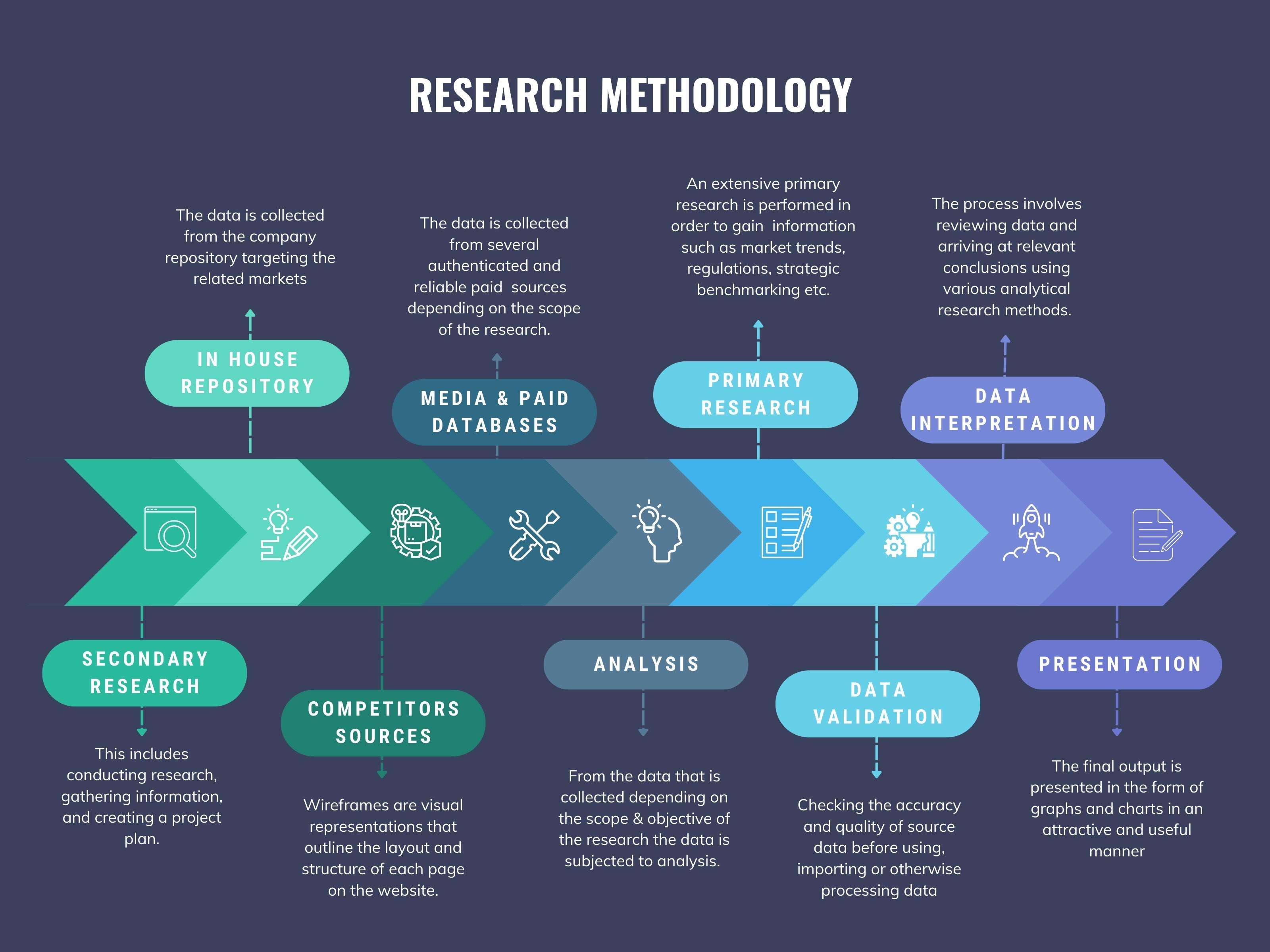
We at ‘Stratistics’ opt for an extensive research approach which involves data mining, data validation, and data analysis. The various research sources include in-house repository, secondary research, competitor’s sources, social media research, client internal data, and primary research.
Our team of analysts prefers the most reliable and authenticated data sources in order to perform the comprehensive literature search. With access to most of the authenticated data bases our team highly considers the best mix of information through various sources to obtain extensive and accurate analysis.
Each report takes an average time of a month and a team of 4 industry analysts. The time may vary depending on the scope and data availability of the desired market report. The various parameters used in the market assessment are standardized in order to enhance the data accuracy.
Data Mining
The data is collected from several authenticated, reliable, paid and unpaid sources and is filtered depending on the scope & objective of the research. Our reports repository acts as an added advantage in this procedure. Data gathering from the raw material suppliers, distributors and the manufacturers is performed on a regular basis, this helps in the comprehensive understanding of the products value chain. Apart from the above mentioned sources the data is also collected from the industry consultants to ensure the objective of the study is in the right direction.
Market trends such as technological advancements, regulatory affairs, market dynamics (Drivers, Restraints, Opportunities and Challenges) are obtained from scientific journals, market related national & international associations and organizations.
Data Analysis
From the data that is collected depending on the scope & objective of the research the data is subjected for the analysis. The critical steps that we follow for the data analysis include:
- Product Lifecycle Analysis
- Competitor analysis
- Risk analysis
- Porters Analysis
- PESTEL Analysis
- SWOT Analysis
The data engineering is performed by the core industry experts considering both the Marketing Mix Modeling and the Demand Forecasting. The marketing mix modeling makes use of multiple-regression techniques to predict the optimal mix of marketing variables. Regression factor is based on a number of variables and how they relate to an outcome such as sales or profits.
Data Validation
The data validation is performed by the exhaustive primary research from the expert interviews. This includes telephonic interviews, focus groups, face to face interviews, and questionnaires to validate our research from all aspects. The industry experts we approach come from the leading firms, involved in the supply chain ranging from the suppliers, distributors to the manufacturers and consumers so as to ensure an unbiased analysis.
We are in touch with more than 15,000 industry experts with the right mix of consultants, CEO's, presidents, vice presidents, managers, experts from both supply side and demand side, executives and so on.
The data validation involves the primary research from the industry experts belonging to:
- Leading Companies
- Suppliers & Distributors
- Manufacturers
- Consumers
- Industry/Strategic Consultants
Apart from the data validation the primary research also helps in performing the fill gap research, i.e. providing solutions for the unmet needs of the research which helps in enhancing the reports quality.
For more details about research methodology, kindly write to us at info@strategymrc.com
Frequently Asked Questions
In case of any queries regarding this report, you can contact the customer service by filing the “Inquiry Before Buy” form available on the right hand side. You may also contact us through email: info@strategymrc.com or phone: +1-301-202-5929
Yes, the samples are available for all the published reports. You can request them by filling the “Request Sample” option available in this page.
Yes, you can request a sample with your specific requirements. All the customized samples will be provided as per the requirement with the real data masked.
All our reports are available in Digital PDF format. In case if you require them in any other formats, such as PPT, Excel etc you can submit a request through “Inquiry Before Buy” form available on the right hand side. You may also contact us through email: info@strategymrc.com or phone: +1-301-202-5929
We offer a free 15% customization with every purchase. This requirement can be fulfilled for both pre and post sale. You may send your customization requirements through email at info@strategymrc.com or call us on +1-301-202-5929.
We have 3 different licensing options available in electronic format.
- Single User Licence: Allows one person, typically the buyer, to have access to the ordered product. The ordered product cannot be distributed to anyone else.
- 2-5 User Licence: Allows the ordered product to be shared among a maximum of 5 people within your organisation.
- Corporate License: Allows the product to be shared among all employees of your organisation regardless of their geographical location.
All our reports are typically be emailed to you as an attachment.
To order any available report you need to register on our website. The payment can be made either through CCAvenue or PayPal payments gateways which accept all international cards.
We extend our support to 6 months post sale. A post sale customization is also provided to cover your unmet needs in the report.
Request Customization
We offer complimentary customization of up to 15% with every purchase. To share your customization requirements, feel free to email us at info@strategymrc.com or call us on +1-301-202-5929. .
Please Note: Customization within the 15% threshold is entirely free of charge. If your request exceeds this limit, we will conduct a feasibility assessment. Following that, a detailed quote and timeline will be provided.
WHY CHOOSE US ?

Assured Quality
Best in class reports with high standard of research integrity

24X7 Research Support
Continuous support to ensure the best customer experience.

Free Customization
Adding more values to your product of interest.

Safe & Secure Access
Providing a secured environment for all online transactions.

Trusted by 600+ Brands
Serving the most reputed brands across the world.