Semiconductor Advanced Packaging Materials Market
Semiconductor Advanced Packaging Materials Market Forecasts to 2034 - Global Analysis By Packaging Technology (Flip-Chip Packaging, Wafer-Level Packaging (WLP) and 2.5D & 3D IC Packaging), Material Type, Application, End User and By Geography

According to Stratistics MRC, the Global Semiconductor Advanced Packaging Materials Market is accounted for $8.7 billion in 2026 and is expected to reach $16.0 billion by 2034 growing at a CAGR of 7.9% during the forecast period. Semiconductor Advanced Packaging Materials include substrates, encapsulation materials, adhesives, underfills, molding compounds, thermal solutions, and interconnect materials essential for modern semiconductor packaging. They facilitate compact designs, efficient electrical connections, heat dissipation, structural protection, and integration of multiple semiconductor components. Material innovation increasingly emphasizes higher thermal performance, reduced signal transmission losses, greater durability, finer-pitch connections, and compatibility with 2.5D and 3D packaging, chiplet architectures, fan-out technologies, and heterogeneous integration for advanced semiconductor systems.
According to the Semiconductor Industry Association (SIA), global semiconductor sales reached $791.7 billion in 2025, increasing 25.6% from $630.5 billion in 2024. This supports the expanding underlying semiconductor industry that drives demand for advanced packaging materials.
Market Dynamics:
Driver:
Rising demand for high-performance semiconductor devices
Increasing requirements for powerful and compact semiconductor systems are supporting growth in the Semiconductor Advanced Packaging Materials Market. Applications such as artificial intelligence, high-performance computing, 5G, automotive electronics, and data centers require packaging solutions that manage high processing loads efficiently. Advanced packaging materials enable better heat dissipation, electrical connectivity, signal transmission, and durability. The expansion of chiplet-based designs, 2.5D and 3D packaging, and heterogeneous integration is also increasing the need for specialized substrates, molding compounds, bonding materials, underfills, and thermal materials.
Restraint:
High material and manufacturing costs
Elevated costs associated with advanced materials and packaging processes can limit market expansion. Manufacturing sophisticated substrates, dielectric layers, adhesives, underfills, encapsulation compounds, and thermal materials requires precise specifications and specialized production capabilities. Complex architectures, including 2.5D, 3D, and chiplet designs, further increase processing, equipment, testing, and quality-control expenses. These cost pressures can create challenges for smaller semiconductor manufacturers and price-sensitive applications. Consequently, companies may continue using conventional packaging materials when performance requirements do not justify the additional expense of advanced solutions.
Opportunity:
Growing adoption of chiplet and 3D packaging
Expanding use of chiplet technologies and three-dimensional packaging offers substantial growth opportunities for advanced packaging materials. Chiplet architectures combine specialized semiconductor dies within one package, while 3D integration increases component density and reduces interconnection distances. Such designs depend on sophisticated substrates, bonding compounds, underfills, dielectric materials, encapsulants, and thermal solutions. Rising development of artificial intelligence processors, high-bandwidth computing systems, and data-center hardware can further increase requirements for innovative materials that deliver compact designs, thermal efficiency, electrical performance, and reliable semiconductor package operation.
Threat:
Rapid technological changes and short product cycles
Fast technological evolution and shortened semiconductor product lifecycles can challenge market stability. Packaging designs are continuously advancing toward greater integration, compact dimensions, and improved performance, creating ongoing requirements for material innovation. Materials suitable for existing packaging generations may need substantial modification when new architectures are introduced. This situation can expose manufacturers to investment risks associated with specialized equipment and research programs. Frequent technology transitions may raise development expenses, reduce product lifetimes, and create uncertainty surrounding sustained demand for particular advanced packaging materials globally.
Covid-19 Impact:
The COVID-19 pandemic affected the Semiconductor Advanced Packaging Materials Market by causing manufacturing shutdowns, labor limitations, logistics disruptions, and shortages across supply networks. Producers faced challenges sourcing substrates, chemicals, adhesives, and other specialized packaging inputs, while transportation restrictions delayed deliveries and manufacturing activities. However, greater demand for computers, connectivity equipment, cloud services, and electronic devices helped sustain semiconductor requirements across multiple applications. Following operational recovery, manufacturers increasingly focused on resilient supply chains, inventory management, and diversified sourcing while continuing investments in advanced packaging technologies worldwide.
The flip-chip packaging segment is expected to be the largest during the forecast period
The flip-chip packaging segment is expected to account for the largest market share during the forecast period. This technology connects semiconductor dies directly to substrates using distributed bump interconnections, enabling compact structures and efficient electrical pathways. Its characteristics support improved signal performance, heat management, high interconnection density, and smaller package footprints. Flip-chip solutions are used across processors, memory products, networking hardware, automotive electronics, and high-performance computing applications. Their broad utilization continues generating demand for advanced substrates, underfills, soldering materials, and protective encapsulation solutions.
The optoelectronics & photonics segment is expected to have the highest CAGR during the forecast period
Over the forecast period, the optoelectronics & photonics segment is predicted to witness the highest growth rate. Its evolving requirements emphasize materials capable of enabling compact integration, efficient heat dissipation, dependable signal transmission, and high-speed optical performance. Combining optical components with semiconductor devices is increasing requirements for specialized substrates, bonding compounds, encapsulation materials, and thermal-management solutions. Expanding applications of photonics across telecommunications, data centers, sensing systems, and high-performance computing are further encouraging innovation and adoption of advanced packaging materials.
Region with largest share:
During the forecast period, the Asia Pacific region is expected to hold the largest market share because of its well-established semiconductor production and packaging infrastructure. Taiwan, China, South Korea, Japan, and Southeast Asia collectively provide important manufacturing, assembly, testing, and materials capabilities. The presence of foundries, OSAT providers, substrate producers, and specialized material suppliers supports an interconnected supply network. Taiwan’s advanced packaging expansion, Japan’s specialized material production, and South Korea’s packaging ecosystem contribute to continued regional demand for substrates, encapsulation materials, bonding solutions, and thermal management products.
Region with highest CAGR:
Over the forecast period, the North America region is anticipated to exhibit the highest CAGR as investments increase across semiconductor production, artificial intelligence, high-performance computing, and advanced packaging infrastructure. Expanding domestic manufacturing programs, demand for advanced processors, and efforts to strengthen regional supply chains are supporting market development. New investments in packaging facilities and associated material technologies are increasing requirements for specialized substrates, bonding compounds, encapsulation materials, underfills, and thermal management solutions, particularly throughout the United States semiconductor and technology ecosystem.
Key players in the market
Some of the key players in Semiconductor Advanced Packaging Materials Market include Ajinomoto Fine-Techno Co., Inc., Henkel AG & Co. KGaA, IBIDEN, LG Chem, Namics Corporation, Nan Ya PCB Co., Ltd., Resonac Holdings Corporation, Samsung Electro-Mechanics, DuPont, Sumitomo Bakelite, Panasonic, Shinko Electric Industries, Unimicron Technology, Toppan, Shin-Etsu Chemical, Mitsui High-tec, Kinsus Interconnect Technology and AT&S.
Key Developments:
In March 2026, Henkel AG has agreed buy Olaplex Holdings Inc., the hair-care brand that developed a cult following for its shampoos and other treatments, in a $1.4 billion deal. Dusseldorf, Germany-based Henkel will pay $2.06 a share for Olaplex.
In September 2025, LG Chem announced that Toyota Tsusho Corporation had acquired a 25% stake in LG-HY BCM, the company’s cathode materials plant in Gumi, thereby joining as the second-largest shareholder. Toyota Tsusho, the general trading company of the Toyota Group, plays a vital role in Toyota Motor’s raw material procurement.
Packaging Technologies Covered:
• Flip-Chip Packaging
• Wafer-Level Packaging (WLP)
• 2.5D & 3D IC Packaging
Material Types Covered:
• Substrates
• Encapsulation Resins
• Underfill Materials
• Solder Balls & Bumps
• Thermal Interface Materials
• Die Attach Materials
• Bonding Wires
Applications Covered:
• Logic & Microprocessors
• Memory Devices
• Analog & Mixed Signal ICs
• RF & Power Devices
• Optoelectronics & Photonics
End Users Covered:
• Consumer Electronics
• Automotive Electronics
• Telecommunications
• Industrial Electronics
• Healthcare & Medical Devices
Regions Covered:
• North America
o United States
o Canada
o Mexico
• Europe
o United Kingdom
o Germany
o France
o Italy
o Spain
o Netherlands
o Belgium
o Sweden
o Switzerland
o Poland
o Rest of Europe
• Asia Pacific
o China
o Japan
o India
o South Korea
o Australia
o Indonesia
o Thailand
o Malaysia
o Singapore
o Vietnam
o Rest of Asia Pacific
• South America
o Brazil
o Argentina
o Colombia
o Chile
o Peru
o Rest of South America
• Rest of the World (RoW)
o Middle East
§ Saudi Arabia
§ United Arab Emirates
§ Qatar
§ Israel
§ Rest of Middle East
o Africa
§ South Africa
§ Egypt
§ Morocco
§ Rest of Africa
What our report offers:
- Market share assessments for the regional and country-level segments
- Strategic recommendations for the new entrants
- Covers Market data for the years 2023, 2024, 2025, 2026, 2027, 2028, 2030, 2032 and 2034
- Market Trends (Drivers, Constraints, Opportunities, Threats, Challenges, Investment Opportunities, and recommendations)
- Strategic recommendations in key business segments based on the market estimations
- Competitive landscaping mapping the key common trends
- Company profiling with detailed strategies, financials, and recent developments
- Supply chain trends mapping the latest technological advancements
Free Customization Offerings:
All the customers of this report will be entitled to receive one of the following free customization options:
• Company Profiling
o Comprehensive profiling of additional market players (up to 3)
o SWOT Analysis of key players (up to 3)
• Regional Segmentation
o Market estimations, Forecasts and CAGR of any prominent country as per the client's interest (Note: Depends on feasibility check)
• Competitive Benchmarking
o Benchmarking of key players based on product portfolio, geographical presence, and strategic alliances
Table of Contents
1 Executive Summary
1.1 Market Snapshot and Key Highlights
1.2 Growth Drivers, Challenges, and Opportunities
1.3 Competitive Landscape Overview
1.4 Strategic Insights and Recommendations
2 Research Framework
2.1 Study Objectives and Scope
2.2 Stakeholder Analysis
2.3 Research Assumptions and Limitations
2.4 Research Methodology
2.4.1 Data Collection (Primary and Secondary)
2.4.2 Data Modeling and Estimation Techniques
2.4.3 Data Validation and Triangulation
2.4.4 Analytical and Forecasting Approach
3 Market Dynamics and Trend Analysis
3.1 Market Definition and Structure
3.2 Key Market Drivers
3.3 Market Restraints and Challenges
3.4 Growth Opportunities and Investment Hotspots
3.5 Industry Threats and Risk Assessment
3.6 Technology and Innovation Landscape
3.7 Emerging and High-Growth Markets
3.8 Regulatory and Policy Environment
3.9 Impact of COVID-19 and Recovery Outlook
4 Competitive and Strategic Assessment
4.1 Porter's Five Forces Analysis
4.1.1 Supplier Bargaining Power
4.1.2 Buyer Bargaining Power
4.1.3 Threat of Substitutes
4.1.4 Threat of New Entrants
4.1.5 Competitive Rivalry
4.2 Market Share Analysis of Key Players
4.3 Product Benchmarking and Performance Comparison
5 Global Semiconductor Advanced Packaging Materials Market, By Packaging Technology
5.1 Flip-Chip Packaging
5.2 Wafer-Level Packaging (WLP)
5.3 2.5D & 3D IC Packaging
6 Global Semiconductor Advanced Packaging Materials Market, By Material Type
6.1 Substrates
6.1.1 Organic
6.1.2 Ceramic
6.1.3 Glass
6.2 Encapsulation Resins
6.3 Underfill Materials
6.4 Solder Balls & Bumps
6.5 Thermal Interface Materials
6.6 Die Attach Materials
6.7 Bonding Wires
7 Global Semiconductor Advanced Packaging Materials Market, By Application
7.1 Logic & Microprocessors
7.2 Memory Devices
7.3 Analog & Mixed Signal ICs
7.4 RF & Power Devices
7.5 Optoelectronics & Photonics
8 Global Semiconductor Advanced Packaging Materials Market, By End User
8.1 Consumer Electronics
8.2 Automotive Electronics
8.3 Telecommunications
8.4 Industrial Electronics
8.5 Healthcare & Medical Devices
9 Global Semiconductor Advanced Packaging Materials Market, By Geography
9.1 North America
9.1.1 United States
9.1.2 Canada
9.1.3 Mexico
9.2 Europe
9.2.1 United Kingdom
9.2.2 Germany
9.2.3 France
9.2.4 Italy
9.2.5 Spain
9.2.6 Netherlands
9.2.7 Belgium
9.2.8 Sweden
9.2.9 Switzerland
9.2.10 Poland
9.2.11 Rest of Europe
9.3 Asia Pacific
9.3.1 China
9.3.2 Japan
9.3.3 India
9.3.4 South Korea
9.3.5 Australia
9.3.6 Indonesia
9.3.7 Thailand
9.3.8 Malaysia
9.3.9 Singapore
9.3.10 Vietnam
9.3.11 Rest of Asia Pacific
9.4 South America
9.4.1 Brazil
9.4.2 Argentina
9.4.3 Colombia
9.4.4 Chile
9.4.5 Peru
9.4.6 Rest of South America
9.5 Rest of the World (RoW)
9.5.1 Middle East
9.5.1.1 Saudi Arabia
9.5.1.2 United Arab Emirates
9.5.1.3 Qatar
9.5.1.4 Israel
9.5.1.5 Rest of Middle East
9.5.2 Africa
9.5.2.1 South Africa
9.5.2.2 Egypt
9.5.2.3 Morocco
9.5.2.4 Rest of Africa
10 Strategic Market Intelligence
10.1 Industry Value Network and Supply Chain Assessment
10.2 White-Space and Opportunity Mapping
10.3 Product Evolution and Market Life Cycle Analysis
10.4 Channel, Distributor, and Go-to-Market Assessment
11 Industry Developments and Strategic Initiatives
11.1 Mergers and Acquisitions
11.2 Partnerships, Alliances, and Joint Ventures
11.3 New Product Launches and Certifications
11.4 Capacity Expansion and Investments
11.5 Other Strategic Initiatives
12 Company Profiles
12.1 Ajinomoto Fine-Techno Co., Inc.
12.2 Henkel AG & Co. KGaA
12.3 IBIDEN
12.4 LG Chem
12.5 Namics Corporation
12.6 Nan Ya PCB Co., Ltd.
12.7 Resonac Holdings Corporation
12.8 Samsung Electro-Mechanics
12.9 DuPont
12.10 Sumitomo Bakelite
12.11 Panasonic
12.12 Shinko Electric Industries
12.13 Unimicron Technology
12.14 Toppan
12.15 Shin-Etsu Chemical
12.16 Mitsui High-tec
12.17 Kinsus Interconnect Technology
12.18 AT&S
List of Tables
1 Global Semiconductor Advanced Packaging Materials Market Outlook, By Region (2023-2034) ($MN)
2 Global Semiconductor Advanced Packaging Materials Market Outlook, By Packaging Technology (2023-2034) ($MN)
3 Global Semiconductor Advanced Packaging Materials Market Outlook, By Flip-Chip Packaging (2023-2034) ($MN)
4 Global Semiconductor Advanced Packaging Materials Market Outlook, By Wafer-Level Packaging (WLP) (2023-2034) ($MN)
5 Global Semiconductor Advanced Packaging Materials Market Outlook, By 2.5D & 3D IC Packaging (2023-2034) ($MN)
6 Global Semiconductor Advanced Packaging Materials Market Outlook, By Material Type (2023-2034) ($MN)
7 Global Semiconductor Advanced Packaging Materials Market Outlook, By Substrates (2023-2034) ($MN)
8 Global Semiconductor Advanced Packaging Materials Market Outlook, By Organic (2023-2034) ($MN)
9 Global Semiconductor Advanced Packaging Materials Market Outlook, By Ceramic (2023-2034) ($MN)
10 Global Semiconductor Advanced Packaging Materials Market Outlook, By Glass (2023-2034) ($MN)
11 Global Semiconductor Advanced Packaging Materials Market Outlook, By Encapsulation Resins (2023-2034) ($MN)
12 Global Semiconductor Advanced Packaging Materials Market Outlook, By Underfill Materials (2023-2034) ($MN)
13 Global Semiconductor Advanced Packaging Materials Market Outlook, By Solder Balls & Bumps (2023-2034) ($MN)
14 Global Semiconductor Advanced Packaging Materials Market Outlook, By Thermal Interface Materials (2023-2034) ($MN)
15 Global Semiconductor Advanced Packaging Materials Market Outlook, By Die Attach Materials (2023-2034) ($MN)
16 Global Semiconductor Advanced Packaging Materials Market Outlook, By Bonding Wires (2023-2034) ($MN)
17 Global Semiconductor Advanced Packaging Materials Market Outlook, By Application (2023-2034) ($MN)
18 Global Semiconductor Advanced Packaging Materials Market Outlook, By Logic & Microprocessors (2023-2034) ($MN)
19 Global Semiconductor Advanced Packaging Materials Market Outlook, By Memory Devices (2023-2034) ($MN)
20 Global Semiconductor Advanced Packaging Materials Market Outlook, By Analog & Mixed Signal ICs (2023-2034) ($MN)
21 Global Semiconductor Advanced Packaging Materials Market Outlook, By RF & Power Devices (2023-2034) ($MN)
22 Global Semiconductor Advanced Packaging Materials Market Outlook, By Optoelectronics & Photonics (2023-2034) ($MN)
23 Global Semiconductor Advanced Packaging Materials Market Outlook, By End User (2023-2034) ($MN)
24 Global Semiconductor Advanced Packaging Materials Market Outlook, By Consumer Electronics (2023-2034) ($MN)
25 Global Semiconductor Advanced Packaging Materials Market Outlook, By Automotive Electronics (2023-2034) ($MN)
26 Global Semiconductor Advanced Packaging Materials Market Outlook, By Telecommunications (2023-2034) ($MN)
27 Global Semiconductor Advanced Packaging Materials Market Outlook, By Industrial Electronics (2023-2034) ($MN)
28 Global Semiconductor Advanced Packaging Materials Market Outlook, By Healthcare & Medical Devices (2023-2034) ($MN)
Note: Tables for North America, Europe, APAC, South America, and Rest of the World (RoW) Regions are also represented in the same manner as above.
List of Figures
RESEARCH METHODOLOGY
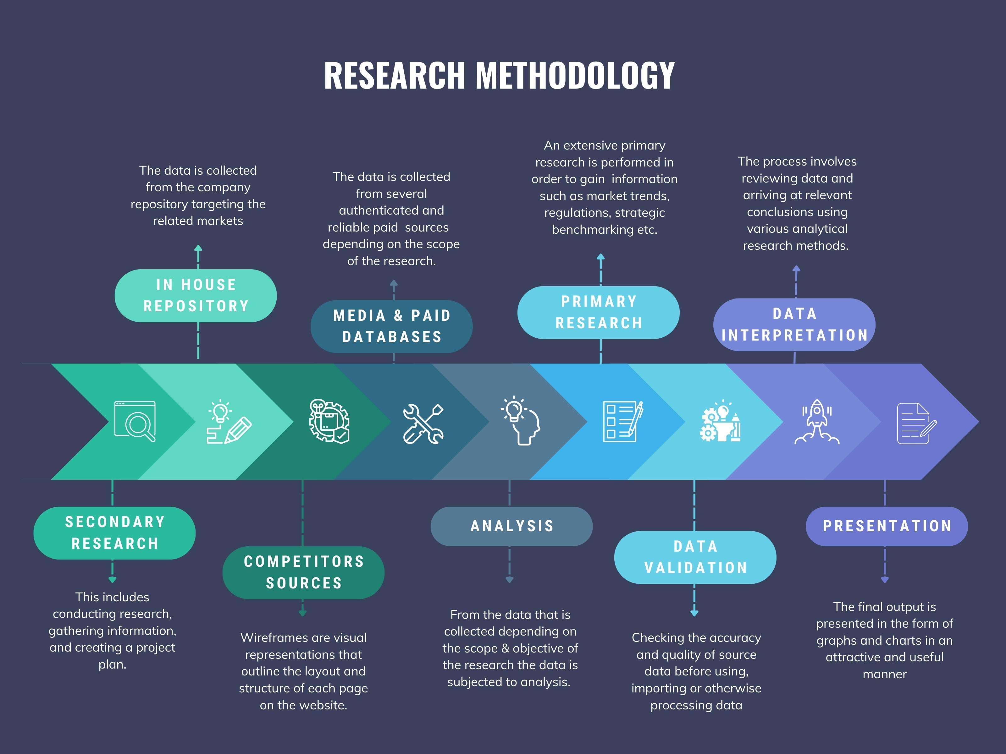
We at ‘Stratistics’ opt for an extensive research approach which involves data mining, data validation, and data analysis. The various research sources include in-house repository, secondary research, competitor’s sources, social media research, client internal data, and primary research.
Our team of analysts prefers the most reliable and authenticated data sources in order to perform the comprehensive literature search. With access to most of the authenticated data bases our team highly considers the best mix of information through various sources to obtain extensive and accurate analysis.
Each report takes an average time of a month and a team of 4 industry analysts. The time may vary depending on the scope and data availability of the desired market report. The various parameters used in the market assessment are standardized in order to enhance the data accuracy.
Data Mining
The data is collected from several authenticated, reliable, paid and unpaid sources and is filtered depending on the scope & objective of the research. Our reports repository acts as an added advantage in this procedure. Data gathering from the raw material suppliers, distributors and the manufacturers is performed on a regular basis, this helps in the comprehensive understanding of the products value chain. Apart from the above mentioned sources the data is also collected from the industry consultants to ensure the objective of the study is in the right direction.
Market trends such as technological advancements, regulatory affairs, market dynamics (Drivers, Restraints, Opportunities and Challenges) are obtained from scientific journals, market related national & international associations and organizations.
Data Analysis
From the data that is collected depending on the scope & objective of the research the data is subjected for the analysis. The critical steps that we follow for the data analysis include:
- Product Lifecycle Analysis
- Competitor analysis
- Risk analysis
- Porters Analysis
- PESTEL Analysis
- SWOT Analysis
The data engineering is performed by the core industry experts considering both the Marketing Mix Modeling and the Demand Forecasting. The marketing mix modeling makes use of multiple-regression techniques to predict the optimal mix of marketing variables. Regression factor is based on a number of variables and how they relate to an outcome such as sales or profits.
Data Validation
The data validation is performed by the exhaustive primary research from the expert interviews. This includes telephonic interviews, focus groups, face to face interviews, and questionnaires to validate our research from all aspects. The industry experts we approach come from the leading firms, involved in the supply chain ranging from the suppliers, distributors to the manufacturers and consumers so as to ensure an unbiased analysis.
We are in touch with more than 15,000 industry experts with the right mix of consultants, CEO's, presidents, vice presidents, managers, experts from both supply side and demand side, executives and so on.
The data validation involves the primary research from the industry experts belonging to:
- Leading Companies
- Suppliers & Distributors
- Manufacturers
- Consumers
- Industry/Strategic Consultants
Apart from the data validation the primary research also helps in performing the fill gap research, i.e. providing solutions for the unmet needs of the research which helps in enhancing the reports quality.
For more details about research methodology, kindly write to us at info@strategymrc.com
Frequently Asked Questions
In case of any queries regarding this report, you can contact the customer service by filing the “Inquiry Before Buy” form available on the right hand side. You may also contact us through email: info@strategymrc.com or phone: +1-301-202-5929
Yes, the samples are available for all the published reports. You can request them by filling the “Request Sample” option available in this page.
Yes, you can request a sample with your specific requirements. All the customized samples will be provided as per the requirement with the real data masked.
All our reports are available in Digital PDF format. In case if you require them in any other formats, such as PPT, Excel etc you can submit a request through “Inquiry Before Buy” form available on the right hand side. You may also contact us through email: info@strategymrc.com or phone: +1-301-202-5929
We offer a free 15% customization with every purchase. This requirement can be fulfilled for both pre and post sale. You may send your customization requirements through email at info@strategymrc.com or call us on +1-301-202-5929.
We have 3 different licensing options available in electronic format.
- Single User Licence: Allows one person, typically the buyer, to have access to the ordered product. The ordered product cannot be distributed to anyone else.
- 2-5 User Licence: Allows the ordered product to be shared among a maximum of 5 people within your organisation.
- Corporate License: Allows the product to be shared among all employees of your organisation regardless of their geographical location.
All our reports are typically be emailed to you as an attachment.
To order any available report you need to register on our website. The payment can be made either through CCAvenue or PayPal payments gateways which accept all international cards.
We extend our support to 6 months post sale. A post sale customization is also provided to cover your unmet needs in the report.
Request Customization
We offer complimentary customization of up to 15% with every purchase. To share your customization requirements, feel free to email us at info@strategymrc.com or call us on +1-301-202-5929. .
Please Note: Customization within the 15% threshold is entirely free of charge. If your request exceeds this limit, we will conduct a feasibility assessment. Following that, a detailed quote and timeline will be provided.
WHY CHOOSE US ?

Assured Quality
Best in class reports with high standard of research integrity

24X7 Research Support
Continuous support to ensure the best customer experience.

Free Customization
Adding more values to your product of interest.

Safe & Secure Access
Providing a secured environment for all online transactions.

Trusted by 600+ Brands
Serving the most reputed brands across the world.