
Advanced Electronic Packaging Materials Market
Advanced Electronic Packaging Materials Market Forecasts To 2034 – Global Analysis By Material Type (Organic Substrates, Ceramic Materials, Glass Materials, Metal Materials, Polymer Materials, Dielectric Materials, Encapsulation & Molding Compounds, Underfill Materials, Solder Materials, Lead Frame Materials and Electromagnetic Interference), Substrate Type, Interconnection Material, Thermal Management Material, Dielectric Material, Semiconductor Nodem, Manufacturing Process, Form, Packaging Technology, Application, End-Use Industry and By Geography

According to Stratistics MRC, the Global Advanced Electronic Packaging Materials Market is accounted for $12.9 billion in 2026 and is expected to reach $20.7 billion by 2034 growing at a CAGR of 6.1% during the forecast period. The Advanced Electronic Packaging Materials Market encompasses advanced material solutions designed to support the assembly, protection, and performance of semiconductor packages and electronic devices. It includes high-performance substrates, encapsulation compounds, die bonding materials, underfill resins, thermal interface materials, solder alloys, bonding wires, and conductive pastes that enhance electrical performance, heat dissipation, and structural durability. Rising adoption of AI processors, high-speed computing systems, 5G communication equipment, electric vehicles, and next-generation semiconductor packaging technologies is accelerating market growth. Ongoing advancements in packaging materials are facilitating greater component density, superior thermal efficiency, increased reliability, and improved overall performance of electronic systems.
Market Dynamics:
Driver:
Increasing Adoption of Artificial Intelligence and High-Performance Computing
Growing deployment of artificial intelligence platforms and high-performance computing systems is creating strong demand for sophisticated electronic packaging materials. Advanced processors require packaging solutions that effectively manage heat, maintain signal quality, and ensure reliable electrical connections under intensive operating conditions. Materials such as thermal interface compounds, advanced laminates, encapsulants, and conductive adhesives play a critical role in supporting increasingly complex chip designs. As cloud infrastructure, enterprise computing, and AI-driven technologies continue to expand, semiconductor manufacturers are focusing on packaging innovations that improve energy efficiency, enhance reliability, extend product lifespan, and enable higher processing capabilities across modern electronic systems.
Restraint:
High Development and Material Costs
Substantial expenses associated with producing advanced electronic packaging materials continue to challenge market expansion. Manufacturing specialized substrates, thermal management compounds, conductive materials, and encapsulation solutions demands advanced processing equipment, premium raw materials, and continuous investment in product innovation. In addition, rigorous testing and certification requirements further increase production costs. Smaller manufacturers often face financial barriers when adopting these high-value materials, limiting broader market penetration. Variations in raw material pricing and increasing operational expenditures also affect profitability, making it difficult for companies to introduce new packaging materials while maintaining competitive pricing and sustainable long-term business growth.
Opportunity:
Advancements in Fan-Out and Wafer-Level Packaging Technologies
Ongoing progress in fan-out and wafer-level semiconductor packaging technologies is expanding growth opportunities for suppliers of advanced electronic packaging materials. These highly integrated packaging approaches depend on specialized dielectric compounds, redistribution materials, molding resins, underfills, and thermal interface solutions that enable compact, high-performance semiconductor devices. Rising implementation across consumer electronics, automotive systems, telecommunications equipment, and wearable devices is increasing the need for innovative material technologies. Continued advancements in semiconductor miniaturization and manufacturing efficiency are expected to create sustained demand for packaging materials that enhance reliability, improve electrical characteristics, and support next-generation electronic products.
Threat:
Increasing Environmental Compliance Requirements
Strengthening environmental legislation and sustainability standards present considerable challenges for companies producing advanced electronic packaging materials. Compliance with evolving regulations concerning hazardous substances, emissions control, recycling, and chemical safety often requires extensive process modifications and ongoing investment in environmentally responsible technologies. Maintaining product quality while satisfying diverse international regulatory frameworks can increase development complexity and manufacturing expenses. Businesses that cannot adapt efficiently risk losing market opportunities, facing legal consequences, or experiencing reputational setbacks. Growing regulatory pressure therefore remains an important threat affecting operational flexibility and long-term competitiveness within the electronic packaging materials industry.
Covid-19 Impact:
The outbreak of COVID-19 created both challenges and growth opportunities for the Advanced Electronic Packaging Materials Market. Early pandemic restrictions disrupted manufacturing operations through plant closures, logistics interruptions, workforce limitations, and shortages of critical raw materials, affecting semiconductor packaging production. At the same time, increased reliance on digital technologies, remote work, virtual learning, and cloud-based services significantly boosted demand for electronic devices and semiconductor components. This supported higher utilization of advanced packaging materials, including substrates, encapsulation compounds, thermal management solutions, and conductive materials. The experience also prompted companies to diversify supply sources, enhance manufacturing flexibility, and improve long-term supply chain resilience.
The Organic Substrates segment is expected to be the largest during the forecast period
The Organic Substrates segment is expected to account for the largest market share during the forecast period, because they are extensively utilized across modern semiconductor packaging applications requiring high reliability, efficient electrical performance, and economical production. These materials are well suited for advanced package architectures by offering dimensional stability, fine-line routing capability, reduced package weight, and compatibility with large-scale manufacturing processes. Their broad use in processors, memory devices, communication chips, automotive electronics, and consumer electronic products continues to support market leadership. Ongoing innovation in semiconductor integration, miniaturized electronics, and next-generation packaging technologies is expected to sustain strong demand for organic substrate materials throughout the forecast period.
The AI Accelerators & GPUs segment is expected to have the highest CAGR during the forecast period
Over the forecast period, the AI Accelerators & GPUs segment is predicted to witness the highest growth rate, driven by increasing deployment of artificial intelligence workloads, large language models, cloud computing platforms, and advanced analytics across global industries. These high-performance processors generate substantial heat and require next-generation packaging materials capable of delivering exceptional thermal dissipation, electrical integrity, and structural stability. Rising demand for AI servers, intelligent edge devices, enterprise computing systems, and accelerated computing platforms is encouraging greater adoption of advanced substrates, encapsulation materials, conductive interconnects, and thermal management solutions. Continuous innovation in AI hardware architecture is expected to further strengthen demand for sophisticated electronic packaging materials throughout the forecast period.
Region with largest share:
During the forecast period, the Asia-Pacific region is expected to hold the largest market share, supported by its dominant position in global semiconductor production and electronic device manufacturing. The region hosts a comprehensive supply chain that includes wafer fabrication facilities, advanced packaging companies, material suppliers, and electronics manufacturers, enabling efficient large-scale production. Continued investments in semiconductor capacity, next-generation packaging technologies, electric vehicles, high-performance computing, and telecommunications infrastructure are strengthening regional demand for advanced packaging materials. Favorable industrial policies, skilled manufacturing capabilities, and expanding technology investments are expected to sustain Asia-Pacific’s leadership throughout the forecast period.
Region with highest CAGR:
Over the forecast period, the North America region is anticipated to exhibit the highest CAGR, supported by rising investments in semiconductor fabrication, research and development, and advanced chip packaging capabilities. Increasing deployment of AI processors, hyperscale data centers, autonomous technologies, next-generation communication systems, and automotive electronics is driving demand for high-performance packaging materials across the region. Strong collaboration between semiconductor manufacturers, material suppliers, technology companies, and research organizations is encouraging continuous innovation in packaging solutions. Expanding manufacturing initiatives and sustained technological advancements are expected to accelerate market growth and strengthen North America's position throughout the forecast period.
Key players in the market
Some of the key players in Advanced Electronic Packaging Materials Market include Shin-Etsu Chemical Co., Ltd., Henkel AG & Co. KGaA, Sumitomo Bakelite Co., Ltd., Namics Corporation, DuPont de Nemours, Inc., Resonac Holdings Corporation, Kyocera Corporation, Mitsubishi Chemical Group Corporation, Panasonic Industry Co., Ltd., Samsung Electro-Mechanics Co., Ltd., LG Innotek Co., Ltd., Ibiden Co., Ltd., Unimicron Technology Corporation, Indium Corporation, MacDermid Alpha Electronics Solutions, Ajinomoto Co., Inc., Toray Industries, Inc. and Sekisui Chemical Co., Ltd.
Key Developments:
In May 2026, Henkel announced the modernization of its Packaging Competence Center, built upon its strategic partnership with Nordmeccanica established in May 2025. The upgraded center integrates Nordmeccanica's advanced coating and laminating equipment to enable joint testing, validation, and scaling of innovative material solutions.
In May 2026, Sumitomo Bakelite announced that it would present three technical papers jointly with universities and research partner companies at the IEEE Electronic Components and Technology Conference (ECTC 2026).
In November 2025, Samsung Electro-Mechanics signed a Memorandum of Understanding (MOU) with Sumitomo Chemical Group to establish a joint venture (JV) for the manufacturing of glass core, a next-generation package substrate material.
Material Types Covered:
• Organic Substrates
• Ceramic Materials
• Glass Materials
• Metal Materials
• Polymer Materials
• Dielectric Materials
• Encapsulation & Molding Compounds
• Underfill Materials
• Solder Materials
• Lead Frame Materials
• Electromagnetic Interference
Substrate Types Covered:
• Laminate Substrates
• Ceramic Substrates
• Lead Frame Substrates
• Flexible Substrates
• Glass Core Substrates
Interconnection Materials Covered:
• Solder Paste
• Solder Balls
• Bonding Wires
• Conductive Films
• Conductive Pastes
• Conductive Adhesives
Thermal Management Materials Covered:
• Thermal Interface Materials
• Heat Spreader Materials
• Heat Sink Materials
• Phase Change Materials
• Thermal Gap Fillers
Dielectric Materials Covered:
• Epoxy-Based Dielectrics
• Polyimide Dielectrics
• Benzocyclobutene
• Polybenzoxazole
• Low-k Dielectric Materials
• Ultra-Low-k Dielectric Materials
Semiconductor Nodes Covered:
• Above 28 nm
• 16–28 nm
• 7–14 nm
• 5 nm and Below
Manufacturing Processes Covered:
• Compression Molding
• Transfer Molding
• Injection Molding
• Electroplating
• Chemical Vapor Deposition
• Physical Vapor Deposition
• Screen Printing
• Additive Manufacturing
Forms Covered:
• Liquid
• Paste
• Film
• Sheet
• Powder
• Wire
• Pellet
Packaging Technologies Covered:
• Wire Bond Packaging
• Flip-Chip Packaging
• Fan-In Wafer-Level Packaging
• Fan-Out Wafer-Level Packaging
• 2.5D Packaging
• 3D Packaging
• System-in-Package
• Package-on-Package
• Embedded Die Packaging
• Chiplet-Based Packaging
Applications Covered:
• Logic Devices
• AI Accelerators & GPUs
• Memory Devices
• Power Semiconductor Devices
• Analog & Mixed-Signal ICs
• RF Devices
• Photonic Devices
• MEMS & Sensors
End-Use Industries Covered:
• Consumer Electronics
• Automotive Electronics
• Telecommunications
• Data Centers & High-Performance Computing
• Industrial Electronics
• Medical Electronics
• Aerospace & Defense
• Energy & Power
Regions Covered:
• North America
o United States
o Canada
o Mexico
• Europe
o United Kingdom
o Germany
o France
o Italy
o Spain
o Netherlands
o Belgium
o Sweden
o Switzerland
o Poland
o Rest of Europe
• Asia Pacific
o China
o Japan
o India
o South Korea
o Australia
o Indonesia
o Thailand
o Malaysia
o Singapore
o Vietnam
o Rest of Asia Pacific
• South America
o Brazil
o Argentina
o Colombia
o Chile
o Peru
o Rest of South America
• Rest of the World (RoW)
o Middle East
§ Saudi Arabia
§ United Arab Emirates
§ Qatar
§ Israel
§ Rest of Middle East
o Africa
§ South Africa
§ Egypt
§ Morocco
§ Rest of Africa
What our report offers:
- Market share assessments for the regional and country-level segments
- Strategic recommendations for the new entrants
- Covers Market data for the years 2023, 2024, 2025, 2026, 2027, 2028, 2030, 2032 and 2034
- Market Trends (Drivers, Constraints, Opportunities, Threats, Challenges, Investment Opportunities, and recommendations)
- Strategic recommendations in key business segments based on the market estimations
- Competitive landscaping mapping the key common trends
- Company profiling with detailed strategies, financials, and recent developments
- Supply chain trends mapping the latest technological advancements
Free Customization Offerings:
All the customers of this report will be entitled to receive one of the following free customization options:
• Company Profiling
o Comprehensive profiling of additional market players (up to 3)
o SWOT Analysis of key players (up to 3)
• Regional Segmentation
o Market estimations, Forecasts and CAGR of any prominent country as per the client's interest (Note: Depends on feasibility check)
• Competitive Benchmarking
o Benchmarking of key players based on product portfolio, geographical presence, and strategic alliances
Table of Contents
1 Executive Summary
1.1 Market Snapshot and Key Highlights
1.2 Growth Drivers, Challenges, and Opportunities
1.3 Competitive Landscape Overview
1.4 Strategic Insights and Recommendations
2 Research Framework
2.1 Study Objectives and Scope
2.2 Stakeholder Analysis
2.3 Research Assumptions and Limitations
2.4 Research Methodology
2.4.1 Data Collection (Primary and Secondary)
2.4.2 Data Modeling and Estimation Techniques
2.4.3 Data Validation and Triangulation
2.4.4 Analytical and Forecasting Approach
3 Market Dynamics and Trend Analysis
3.1 Market Definition and Structure
3.2 Key Market Drivers
3.3 Market Restraints and Challenges
3.4 Growth Opportunities and Investment Hotspots
3.5 Industry Threats and Risk Assessment
3.6 Technology and Innovation Landscape
3.7 Emerging and High-Growth Markets
3.8 Regulatory and Policy Environment
3.9 Impact of COVID-19 and Recovery Outlook
4 Competitive and Strategic Assessment
4.1 Porter's Five Forces Analysis
4.1.1 Supplier Bargaining Power
4.1.2 Buyer Bargaining Power
4.1.3 Threat of Substitutes
4.1.4 Threat of New Entrants
4.1.5 Competitive Rivalry
4.2 Market Share Analysis of Key Players
4.3 Product Benchmarking and Performance Comparison
5 Global Advanced Electronic Packaging Materials Market, By Material Type
5.1 Organic Substrates
5.2 Ceramic Materials
5.3 Glass Materials
5.4 Metal Materials
5.5 Polymer Materials
5.6 Dielectric Materials
5.7 Encapsulation & Molding Compounds
5.8 Underfill Materials
5.9 Solder Materials
5.10 Lead Frame Materials
5.11 Electromagnetic Interference
6 Global Advanced Electronic Packaging Materials Market, By Substrate Type
6.1 Laminate Substrates
6.2 Ceramic Substrates
6.3 Lead Frame Substrates
6.4 Flexible Substrates
6.5 Glass Core Substrates
7 Global Advanced Electronic Packaging Materials Market, By Interconnection Material
7.1 Solder Paste
7.2 Solder Balls
7.3 Bonding Wires
7.4 Conductive Films
7.5 Conductive Pastes
7.6 Conductive Adhesives
8 Global Advanced Electronic Packaging Materials Market, By Thermal Management Material
8.1 Thermal Interface Materials
8.2 Heat Spreader Materials
8.3 Heat Sink Materials
8.4 Phase Change Materials
8.5 Thermal Gap Fillers
9 Global Advanced Electronic Packaging Materials Market, By Dielectric Material
9.1 Epoxy-Based Dielectrics
9.2 Polyimide Dielectrics
9.3 Benzocyclobutene
9.4 Polybenzoxazole
9.5 Low-k Dielectric Materials
9.6 Ultra-Low-k Dielectric Materials
10 Global Advanced Electronic Packaging Materials Market, By Semiconductor Node
10.1 Above 28 nm
10.2 16–28 nm
10.3 7–14 nm
10.4 5 nm and Below
11 Global Advanced Electronic Packaging Materials Market, By Manufacturing Process
11.1 Compression Molding
11.2 Transfer Molding
11.3 Injection Molding
11.4 Electroplating
11.5 Chemical Vapor Deposition
11.6 Physical Vapor Deposition
11.7 Screen Printing
11.8 Additive Manufacturing
12 Global Advanced Electronic Packaging Materials Market, By Form
12.1 Liquid
12.2 Paste
12.3 Film
12.4 Sheet
12.5 Powder
12.6 Wire
12.7 Pellet
13 Global Advanced Electronic Packaging Materials Market, By Packaging Technology
13.1 Wire Bond Packaging
13.2 Flip-Chip Packaging
13.3 Fan-In Wafer-Level Packaging
13.4 Fan-Out Wafer-Level Packaging
13.5 2.5D Packaging
13.6 3D Packaging
13.7 System-in-Package
13.8 Package-on-Package
13.9 Embedded Die Packaging
13.10 Chiplet-Based Packaging
14 Global Advanced Electronic Packaging Materials Market, By Application
14.1 Logic Devices
14.2 AI Accelerators & GPUs
14.3 Memory Devices
14.4 Power Semiconductor Devices
14.5 Analog & Mixed-Signal ICs
14.6 RF Devices
14.7 Photonic Devices
14.8 MEMS & Sensors
15 Global Advanced Electronic Packaging Materials Market, By End-Use Industry
15.1 Consumer Electronics
15.2 Automotive Electronics
15.3 Telecommunications
15.4 Data Centers & High-Performance Computing
15.5 Industrial Electronics
15.6 Medical Electronics
15.7 Aerospace & Defense
15.8 Energy & Power
16 Global Advanced Electronic Packaging Materials Market, By Geography
16.1 North America
16.1.1 United States
16.1.2 Canada
16.1.3 Mexico
16.2.1 Europe
16.2.1 United Kingdom
16.2.2 Germany
16.2.3 France
16.2.4 Italy
16.2.5 Spain
16.2.6 Netherlands
16.2.7 Belgium
16.2.8 Sweden
16.2.9 Switzerland
16.2.10 Poland
16.2.11 Rest of Europe
16.3 Asia Pacific
16.3.1 China
16.3.2 Japan
16.3.3 India
16.3.4 South Korea
16.3.5 Australia
16.3.6 Indonesia
16.3.7 Thailand
16.3.8 Malaysia
16.3.9 Singapore
16.3.10 Vietnam
16.3.11 Rest of Asia Pacific
16.4 South America
16.4.1 Brazil
16.4.2 Argentina
16.4.3 Colombia
16.4.4 Chile
16.4.5 Peru
16.4.6 Rest of South America
16.5 Rest of the World (RoW)
16.5.1 Middle East
16.5.1.1 Saudi Arabia
16.5.1.2 United Arab Emirates
16.5.1.3 Qatar
16.5.1.4 Israel
16.5.1.5 Rest of Middle East
16.5.2 Africa
16.5.2.1 South Africa
16.5.2.2 Egypt
16.5.2.3 Morocco
16.5.2.4 Rest of Africa
17 Strategic Market Intelligence
17.1 Industry Value Network and Supply Chain Assessment
17.2 White-Space and Opportunity Mapping
17.3 Product Evolution and Market Life Cycle Analysis
17.4 Channel, Distributor, and Go-to-Market Assessment
18 Industry Developments and Strategic Initiatives
18.1 Mergers and Acquisitions
18.2 Partnerships, Alliances, and Joint Ventures
18.3 New Product Launches and Certifications
18.4 Capacity Expansion and Investments
18.5 Other Strategic Initiatives
19 Company Profiles
19.1 Shin-Etsu Chemical Co., Ltd.
19.2 Henkel AG & Co. KGaA
19.3 Sumitomo Bakelite Co., Ltd.
19.4 Namics Corporation
19.5 DuPont de Nemours, Inc.
19.6 Resonac Holdings Corporation
19.7 Kyocera Corporation
19.8 Mitsubishi Chemical Group Corporation
19.9 Panasonic Industry Co., Ltd.
19.10 Samsung Electro-Mechanics Co., Ltd.
19.11 LG Innotek Co., Ltd.
19.12 Ibiden Co., Ltd.
19.13 Unimicron Technology Corporation
19.14 Indium Corporation
19.15 MacDermid Alpha Electronics Solutions
19.16 Ajinomoto Co., Inc.
19.17 Toray Industries, Inc.
19.18 Sekisui Chemical Co., Ltd.
List of Tables
1 Global Advanced Electronic Packaging Materials Market Outlook, By Region (2023-2034) ($MN)
2 Global Advanced Electronic Packaging Materials Market Outlook, By Material Type (2023-2034) ($MN)
3 Global Advanced Electronic Packaging Materials Market Outlook, By Organic Substrates (2023-2034) ($MN)
4 Global Advanced Electronic Packaging Materials Market Outlook, By Ceramic Materials (2023-2034) ($MN)
5 Global Advanced Electronic Packaging Materials Market Outlook, By Glass Materials (2023-2034) ($MN)
6 Global Advanced Electronic Packaging Materials Market Outlook, By Metal Materials (2023-2034) ($MN)
7 Global Advanced Electronic Packaging Materials Market Outlook, By Polymer Materials (2023-2034) ($MN)
8 Global Advanced Electronic Packaging Materials Market Outlook, By Dielectric Materials (2023-2034) ($MN)
9 Global Advanced Electronic Packaging Materials Market Outlook, By Encapsulation & Molding Compounds (2023-2034) ($MN)
10 Global Advanced Electronic Packaging Materials Market Outlook, By Underfill Materials (2023-2034) ($MN)
11 Global Advanced Electronic Packaging Materials Market Outlook, By Solder Materials (2023-2034) ($MN)
12 Global Advanced Electronic Packaging Materials Market Outlook, By Lead Frame Materials (2023-2034) ($MN)
13 Global Advanced Electronic Packaging Materials Market Outlook, By Electromagnetic Interference (2023-2034) ($MN)
14 Global Advanced Electronic Packaging Materials Market Outlook, By Substrate Type (2023-2034) ($MN)
15 Global Advanced Electronic Packaging Materials Market Outlook, By Laminate Substrates (2023-2034) ($MN)
16 Global Advanced Electronic Packaging Materials Market Outlook, By Ceramic Substrates (2023-2034) ($MN)
17 Global Advanced Electronic Packaging Materials Market Outlook, By Lead Frame Substrates (2023-2034) ($MN)
18 Global Advanced Electronic Packaging Materials Market Outlook, By Flexible Substrates (2023-2034) ($MN)
19 Global Advanced Electronic Packaging Materials Market Outlook, By Glass Core Substrates (2023-2034) ($MN)
20 Global Advanced Electronic Packaging Materials Market Outlook, By Interconnection Material (2023-2034) ($MN)
21 Global Advanced Electronic Packaging Materials Market Outlook, By Solder Paste (2023-2034) ($MN)
22 Global Advanced Electronic Packaging Materials Market Outlook, By Solder Balls (2023-2034) ($MN)
23 Global Advanced Electronic Packaging Materials Market Outlook, By Bonding Wires (2023-2034) ($MN)
24 Global Advanced Electronic Packaging Materials Market Outlook, By Conductive Films (2023-2034) ($MN)
25 Global Advanced Electronic Packaging Materials Market Outlook, By Conductive Pastes (2023-2034) ($MN)
26 Global Advanced Electronic Packaging Materials Market Outlook, By Conductive Adhesives (2023-2034) ($MN)
27 Global Advanced Electronic Packaging Materials Market Outlook, By Thermal Management Material (2023-2034) ($MN)
28 Global Advanced Electronic Packaging Materials Market Outlook, By Thermal Interface Materials (2023-2034) ($MN)
29 Global Advanced Electronic Packaging Materials Market Outlook, By Heat Spreader Materials (2023-2034) ($MN)
30 Global Advanced Electronic Packaging Materials Market Outlook, By Heat Sink Materials (2023-2034) ($MN)
31 Global Advanced Electronic Packaging Materials Market Outlook, By Phase Change Materials (2023-2034) ($MN)
32 Global Advanced Electronic Packaging Materials Market Outlook, By Thermal Gap Fillers (2023-2034) ($MN)
33 Global Advanced Electronic Packaging Materials Market Outlook, By Dielectric Material (2023-2034) ($MN)
34 Global Advanced Electronic Packaging Materials Market Outlook, By Epoxy-Based Dielectrics (2023-2034) ($MN)
35 Global Advanced Electronic Packaging Materials Market Outlook, By Polyimide Dielectrics (2023-2034) ($MN)
36 Global Advanced Electronic Packaging Materials Market Outlook, By Benzocyclobutene (2023-2034) ($MN)
37 Global Advanced Electronic Packaging Materials Market Outlook, By Polybenzoxazole (2023-2034) ($MN)
38 Global Advanced Electronic Packaging Materials Market Outlook, By Low-k Dielectric Materials (2023-2034) ($MN)
39 Global Advanced Electronic Packaging Materials Market Outlook, By Ultra-Low-k Dielectric Materials (2023-2034) ($MN)
40 Global Advanced Electronic Packaging Materials Market Outlook, By Semiconductor Node (2023-2034) ($MN)
41 Global Advanced Electronic Packaging Materials Market Outlook, By Above 28 nm (2023-2034) ($MN)
42 Global Advanced Electronic Packaging Materials Market Outlook, By 16–28 nm (2023-2034) ($MN)
43 Global Advanced Electronic Packaging Materials Market Outlook, By 7–14 nm (2023-2034) ($MN)
44 Global Advanced Electronic Packaging Materials Market Outlook, By 5 nm and Below (2023-2034) ($MN)
45 Global Advanced Electronic Packaging Materials Market Outlook, By Manufacturing Process (2023-2034) ($MN)
46 Global Advanced Electronic Packaging Materials Market Outlook, By Compression Molding (2023-2034) ($MN)
47 Global Advanced Electronic Packaging Materials Market Outlook, By Transfer Molding (2023-2034) ($MN)
48 Global Advanced Electronic Packaging Materials Market Outlook, By Injection Molding (2023-2034) ($MN)
49 Global Advanced Electronic Packaging Materials Market Outlook, By Electroplating (2023-2034) ($MN)
50 Global Advanced Electronic Packaging Materials Market Outlook, By Chemical Vapor Deposition (2023-2034) ($MN)
51 Global Advanced Electronic Packaging Materials Market Outlook, By Physical Vapor Deposition (2023-2034) ($MN)
52 Global Advanced Electronic Packaging Materials Market Outlook, By Screen Printing (2023-2034) ($MN)
53 Global Advanced Electronic Packaging Materials Market Outlook, By Additive Manufacturing (2023-2034) ($MN)
54 Global Advanced Electronic Packaging Materials Market Outlook, By Form (2023-2034) ($MN)
55 Global Advanced Electronic Packaging Materials Market Outlook, By Liquid (2023-2034) ($MN)
56 Global Advanced Electronic Packaging Materials Market Outlook, By Paste (2023-2034) ($MN)
57 Global Advanced Electronic Packaging Materials Market Outlook, By Film (2023-2034) ($MN)
58 Global Advanced Electronic Packaging Materials Market Outlook, By Sheet (2023-2034) ($MN)
59 Global Advanced Electronic Packaging Materials Market Outlook, By Powder (2023-2034) ($MN)
60 Global Advanced Electronic Packaging Materials Market Outlook, By Wire (2023-2034) ($MN)
61 Global Advanced Electronic Packaging Materials Market Outlook, By Pellet (2023-2034) ($MN)
62 Global Advanced Electronic Packaging Materials Market Outlook, By Packaging Technology (2023-2034) ($MN)
63 Global Advanced Electronic Packaging Materials Market Outlook, By Wire Bond Packaging (2023-2034) ($MN)
64 Global Advanced Electronic Packaging Materials Market Outlook, By Flip-Chip Packaging (2023-2034) ($MN)
65 Global Advanced Electronic Packaging Materials Market Outlook, By Fan-In Wafer-Level Packaging (2023-2034) ($MN)
66 Global Advanced Electronic Packaging Materials Market Outlook, By Fan-Out Wafer-Level Packaging (2023-2034) ($MN)
67 Global Advanced Electronic Packaging Materials Market Outlook, By 2.5D Packaging (2023-2034) ($MN)
68 Global Advanced Electronic Packaging Materials Market Outlook, By 3D Packaging (2023-2034) ($MN)
69 Global Advanced Electronic Packaging Materials Market Outlook, By System-in-Package (2023-2034) ($MN)
70 Global Advanced Electronic Packaging Materials Market Outlook, By Package-on-Package (2023-2034) ($MN)
71 Global Advanced Electronic Packaging Materials Market Outlook, By Embedded Die Packaging (2023-2034) ($MN)
72 Global Advanced Electronic Packaging Materials Market Outlook, By Chiplet-Based Packaging (2023-2034) ($MN)
73 Global Advanced Electronic Packaging Materials Market Outlook, By Application (2023-2034) ($MN)
74 Global Advanced Electronic Packaging Materials Market Outlook, By Logic Devices (2023-2034) ($MN)
75 Global Advanced Electronic Packaging Materials Market Outlook, By AI Accelerators & GPUs (2023-2034) ($MN)
76 Global Advanced Electronic Packaging Materials Market Outlook, By Memory Devices (2023-2034) ($MN)
77 Global Advanced Electronic Packaging Materials Market Outlook, By Power Semiconductor Devices (2023-2034) ($MN)
78 Global Advanced Electronic Packaging Materials Market Outlook, By Analog & Mixed-Signal ICs (2023-2034) ($MN)
79 Global Advanced Electronic Packaging Materials Market Outlook, By RF Devices (2023-2034) ($MN)
80 Global Advanced Electronic Packaging Materials Market Outlook, By Photonic Devices (2023-2034) ($MN)
81 Global Advanced Electronic Packaging Materials Market Outlook, By MEMS & Sensors (2023-2034) ($MN)
82 Global Advanced Electronic Packaging Materials Market Outlook, By End-Use Industry (2023-2034) ($MN)
83 Global Advanced Electronic Packaging Materials Market Outlook, By Consumer Electronics (2023-2034) ($MN)
84 Global Advanced Electronic Packaging Materials Market Outlook, By Automotive Electronics (2023-2034) ($MN)
85 Global Advanced Electronic Packaging Materials Market Outlook, By Telecommunications (2023-2034) ($MN)
86 Global Advanced Electronic Packaging Materials Market Outlook, By Data Centers & High-Performance Computing (2023-2034) ($MN)
87 Global Advanced Electronic Packaging Materials Market Outlook, By Industrial Electronics (2023-2034) ($MN)
88 Global Advanced Electronic Packaging Materials Market Outlook, By Medical Electronics (2023-2034) ($MN)
89 Global Advanced Electronic Packaging Materials Market Outlook, By Aerospace & Defense (2023-2034) ($MN)
90 Global Advanced Electronic Packaging Materials Market Outlook, By Energy & Power (2023-2034) ($MN)
Note: Tables for North America, Europe, APAC, South America, and Rest of the World (RoW) Regions are also represented in the same manner as above.
List of Figures
RESEARCH METHODOLOGY
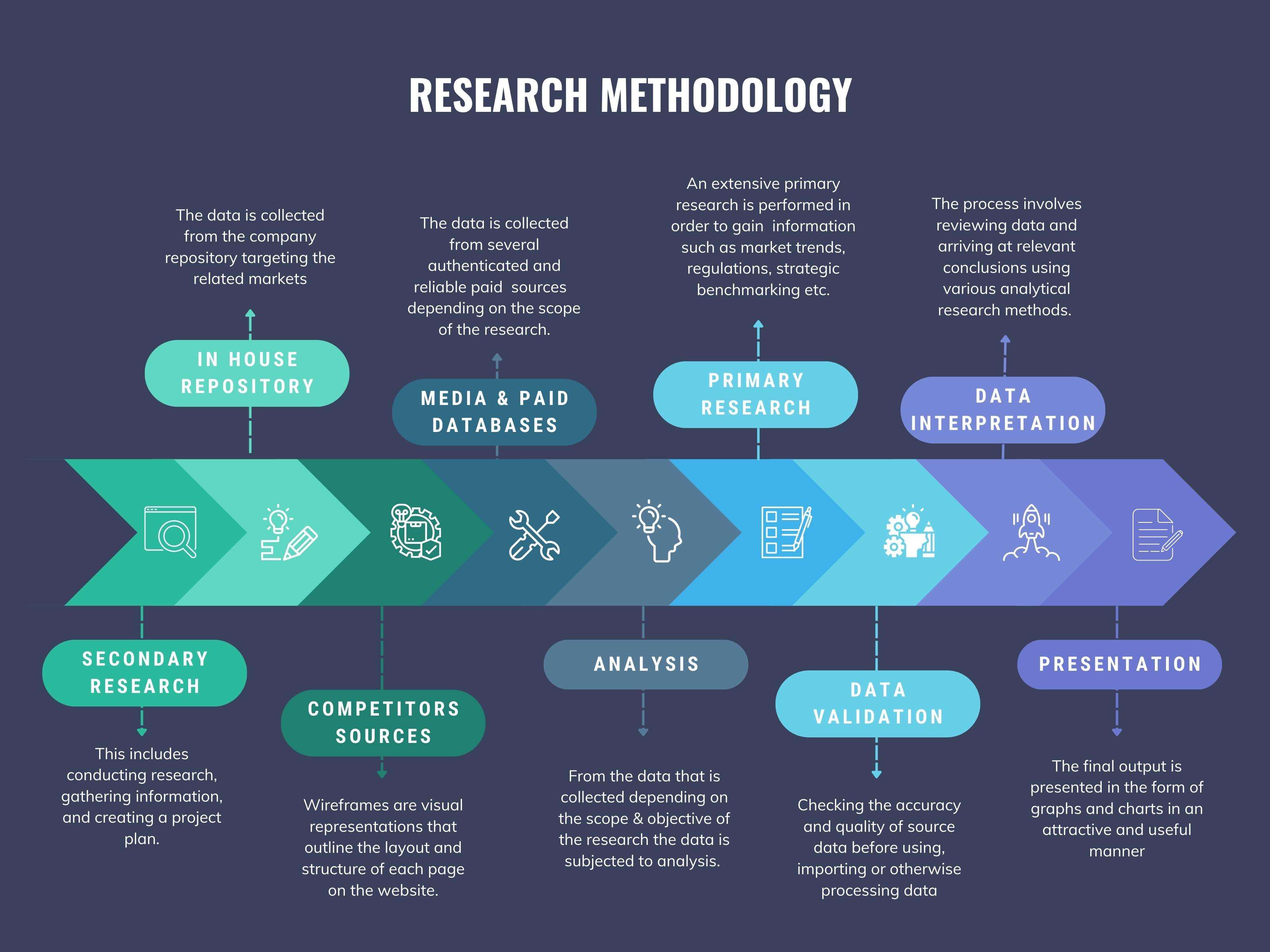
We at ‘Stratistics’ opt for an extensive research approach which involves data mining, data validation, and data analysis. The various research sources include in-house repository, secondary research, competitor’s sources, social media research, client internal data, and primary research.
Our team of analysts prefers the most reliable and authenticated data sources in order to perform the comprehensive literature search. With access to most of the authenticated data bases our team highly considers the best mix of information through various sources to obtain extensive and accurate analysis.
Each report takes an average time of a month and a team of 4 industry analysts. The time may vary depending on the scope and data availability of the desired market report. The various parameters used in the market assessment are standardized in order to enhance the data accuracy.
Data Mining
The data is collected from several authenticated, reliable, paid and unpaid sources and is filtered depending on the scope & objective of the research. Our reports repository acts as an added advantage in this procedure. Data gathering from the raw material suppliers, distributors and the manufacturers is performed on a regular basis, this helps in the comprehensive understanding of the products value chain. Apart from the above mentioned sources the data is also collected from the industry consultants to ensure the objective of the study is in the right direction.
Market trends such as technological advancements, regulatory affairs, market dynamics (Drivers, Restraints, Opportunities and Challenges) are obtained from scientific journals, market related national & international associations and organizations.
Data Analysis
From the data that is collected depending on the scope & objective of the research the data is subjected for the analysis. The critical steps that we follow for the data analysis include:
- Product Lifecycle Analysis
- Competitor analysis
- Risk analysis
- Porters Analysis
- PESTEL Analysis
- SWOT Analysis
The data engineering is performed by the core industry experts considering both the Marketing Mix Modeling and the Demand Forecasting. The marketing mix modeling makes use of multiple-regression techniques to predict the optimal mix of marketing variables. Regression factor is based on a number of variables and how they relate to an outcome such as sales or profits.
Data Validation
The data validation is performed by the exhaustive primary research from the expert interviews. This includes telephonic interviews, focus groups, face to face interviews, and questionnaires to validate our research from all aspects. The industry experts we approach come from the leading firms, involved in the supply chain ranging from the suppliers, distributors to the manufacturers and consumers so as to ensure an unbiased analysis.
We are in touch with more than 15,000 industry experts with the right mix of consultants, CEO's, presidents, vice presidents, managers, experts from both supply side and demand side, executives and so on.
The data validation involves the primary research from the industry experts belonging to:
- Leading Companies
- Suppliers & Distributors
- Manufacturers
- Consumers
- Industry/Strategic Consultants
Apart from the data validation the primary research also helps in performing the fill gap research, i.e. providing solutions for the unmet needs of the research which helps in enhancing the reports quality.
For more details about research methodology, kindly write to us at info@strategymrc.com
Frequently Asked Questions
In case of any queries regarding this report, you can contact the customer service by filing the “Inquiry Before Buy” form available on the right hand side. You may also contact us through email: info@strategymrc.com or phone: +1-301-202-5929
Yes, the samples are available for all the published reports. You can request them by filling the “Request Sample” option available in this page.
Yes, you can request a sample with your specific requirements. All the customized samples will be provided as per the requirement with the real data masked.
All our reports are available in Digital PDF format. In case if you require them in any other formats, such as PPT, Excel etc you can submit a request through “Inquiry Before Buy” form available on the right hand side. You may also contact us through email: info@strategymrc.com or phone: +1-301-202-5929
We offer a free 15% customization with every purchase. This requirement can be fulfilled for both pre and post sale. You may send your customization requirements through email at info@strategymrc.com or call us on +1-301-202-5929.
We have 3 different licensing options available in electronic format.
- Single User Licence: Allows one person, typically the buyer, to have access to the ordered product. The ordered product cannot be distributed to anyone else.
- 2-5 User Licence: Allows the ordered product to be shared among a maximum of 5 people within your organisation.
- Corporate License: Allows the product to be shared among all employees of your organisation regardless of their geographical location.
All our reports are typically be emailed to you as an attachment.
To order any available report you need to register on our website. The payment can be made either through CCAvenue or PayPal payments gateways which accept all international cards.
We extend our support to 6 months post sale. A post sale customization is also provided to cover your unmet needs in the report.
Request Customization
We offer complimentary customization of up to 15% with every purchase. To share your customization requirements, feel free to email us at info@strategymrc.com or call us on +1-301-202-5929. .
Please Note: Customization within the 15% threshold is entirely free of charge. If your request exceeds this limit, we will conduct a feasibility assessment. Following that, a detailed quote and timeline will be provided.
WHY CHOOSE US ?

Assured Quality
Best in class reports with high standard of research integrity

24X7 Research Support
Continuous support to ensure the best customer experience.

Free Customization
Adding more values to your product of interest.

Safe & Secure Access
Providing a secured environment for all online transactions.

Trusted by 600+ Brands
Serving the most reputed brands across the world.