
Sub Nanometer Process Control Market
Sub-Nanometer Process Control Market Forecasts to 2032 – Global Analysis By Control Technique (Lithography Process Control, Etch Process Control, Deposition Process Control, Metrology-Based Control and Real-Time Feedback Control), Node, Measurement Dimension, Application, End User and By Geography

According to Stratistics MRC, the Global Sub-Nanometer Process Control Market is accounted for $7.5 billion in 2025 and is expected to reach $13.1 billion by 2032 growing at a CAGR of 8.1% during the forecast period. Sub-Nanometer Process Control involves precision manufacturing techniques that achieve tolerances smaller than one nanometer. It is critical in semiconductor fabrication, nanotechnology, and advanced optics, where atomic-scale accuracy determines product performance. Using tools like atomic force microscopy, electron beam lithography, and AI-driven monitoring, engineers control deposition, etching, and alignment with extreme precision. This ensures defect-free structures, higher yields, and breakthrough miniaturization. The purpose is to push technological boundaries by enabling reliable production of ultra-small, high-performance devices at the atomic and molecular scale.
Market Dynamics:
Driver:
Advancement toward sub-3nm nodes
Continued scaling of semiconductor devices toward sub-3nm technology nodes is significantly increasing demand for ultra-precise process control solutions. At these dimensions, atomic-level variations can directly impact device performance, power efficiency, and yield. Manufacturers require advanced control systems to manage lithography, etching, and deposition with extreme accuracy. As leading foundries race to commercialize next-generation nodes, investments in sub-nanometer process control technologies become essential to maintain production stability and competitive advantage.
Restraint:
Extremely high equipment costs
Sub-nanometer process control relies on highly specialized metrology tools, advanced lithography systems, and real-time analytics platforms, all of which carry substantial capital costs. Acquisition and maintenance of these systems significantly increase fab operating expenses. Smaller manufacturers and mature-node fabs may struggle to justify such investments. Additionally, frequent tool upgrades required to support node transitions further elevate costs. These financial barriers restrict adoption primarily to large, well-capitalized semiconductor manufacturers operating at advanced technology nodes.
Opportunity:
Advanced process monitoring analytics
Growing adoption of advanced process monitoring and analytics presents a strong opportunity for the sub-nanometer process control market. Integration of AI and machine learning enables early detection of process drifts and defect patterns across complex fabrication steps. Predictive analytics support proactive adjustments, reducing yield loss and downtime. As data volumes within fabs increase, demand for intelligent analytics platforms capable of real-time decision-making continues to rise, positioning process control solutions as critical components of smart semiconductor manufacturing environments.
Threat:
Process variability and yield losses
Increased process variability at sub-nanometer scales poses a major threat to consistent production yields. Minor fluctuations in materials, equipment conditions, or environmental factors can lead to significant defects. Managing variability across multiple tools and process steps becomes increasingly complex as nodes shrink. Failure to maintain tight control can result in yield losses and increased scrap rates. Persistent variability challenges may delay node ramp-ups and undermine confidence in advanced manufacturing processes.
Covid-19 Impact:
The COVID-19 pandemic disrupted global semiconductor equipment supply chains and delayed installation of advanced process control tools. Travel restrictions limited on-site tool calibration and maintenance activities. However, demand for semiconductors surged across digital infrastructure, automotive, and consumer electronics sectors, reinforcing the need for yield optimization. Post-pandemic recovery accelerated investments in advanced fabs and process automation, supporting renewed demand for sub-nanometer process control technologies as manufacturers expand capacity and transition to leading-edge nodes.
The lithography process control segment is expected to be the largest during the forecast period
The lithography process control segment is expected to account for the largest market share during the forecast period, owing to its critical role in defining device patterns at sub-nanometer scales. Precise control of exposure, alignment, and focus is essential for maintaining pattern fidelity. As EUV lithography adoption increases, demand for advanced control and monitoring systems grows. Lithography remains the most process-sensitive step, driving dominant investment in control solutions.
The critical dimension (CD) control segment is expected to have the highest CAGR during the forecast period
Over the forecast period, the critical dimension (CD) control segment is predicted to witness the highest growth rate, impelled by the need to tightly regulate feature sizes at advanced nodes. CD variations directly affect transistor performance and yield. Advanced CD measurement and control tools enable real-time feedback and corrective actions. As device geometries shrink further, fabs increasingly prioritize CD control technologies, driving rapid adoption and high growth rates within this segment.
Region with largest share:
During the forecast period, the Asia Pacific region is expected to hold the largest market share, driven by concentration of leading semiconductor manufacturing hubs. Foundries and IDMs in Taiwan, South Korea, China, and Japan are heavily investing in advanced node production. Continuous fab expansions and government support for semiconductor self-reliance strengthen regional demand. High production volumes and competitive manufacturing environments position Asia Pacific as the dominant market for sub-nanometer process control solutions.
Region with highest CAGR:
Over the forecast period, the North America region is anticipated to exhibit the highest CAGR, attributed to increased investments in domestic semiconductor manufacturing and advanced R&D. Government incentives supporting fab construction and technology development are accelerating adoption of advanced process control tools. Strong presence of semiconductor equipment suppliers and analytics providers supports rapid innovation. Focus on leading-edge nodes and specialty applications positions North America for accelerated growth in sub-nanometer process control technologies.
Key players in the market
Some of the key players in Sub-Nanometer Process Control Market include ASML Holding N.V., KLA Corporation, Applied Materials, Inc., Lam Research Corporation, Tokyo Electron Limited, Hitachi High-Tech Corporation, Onto Innovation Inc., Ultra Clean Holdings, Inc., Advantest Corporation, Brooks Automation, Inc., Teradyne, Inc., Nikon Corporation, Rudolph Technologies, Nordson Corporation and Zeta Technology.
Key Developments:
In December 2025, KLA Corporation introduced AI-powered sub-nanometer process control solutions, providing real-time defect detection, predictive analytics, and yield optimization for advanced semiconductor fabrication.
In November 2025, Applied Materials, Inc. deployed sub-nanometer process control platforms integrating inline metrology, process monitoring, and AI-driven analytics to improve wafer-level precision and manufacturing efficiency.
In October 2025, Lam Research Corporation launched advanced sub-nanometer process monitoring solutions, enabling precise etch and deposition control, defect minimization, and enhanced yield in semiconductor manufacturing.
Control Techniques Covered:
• Lithography Process Control
• Etch Process Control
• Deposition Process Control
• Metrology-Based Control
• Real-Time Feedback Control
Nodes Covered:
• 5nm & Above
• 3nm Node
• 2nm Node
• Below 2nm Node
• Research Nodes
Measurement Dimensions Covered:
• Critical Dimension (CD) Control
• Overlay & Alignment Control
• Film Thickness Control
• Surface Roughness Control
• Line Edge & Line Width Roughness Control
Applications Covered:
• Logic Devices
• Memory Devices
• Power Semiconductors
• Advanced Packaging
• Quantum Devices
End Users Covered:
• Semiconductor Foundries
• IDMs
• Equipment Suppliers
• R&D Centers
• Government Labs
Regions Covered:
• North America
o US
o Canada
o Mexico
• Europe
o Germany
o UK
o Italy
o France
o Spain
o Rest of Europe
• Asia Pacific
o Japan
o China
o India
o Australia
o New Zealand
o South Korea
o Rest of Asia Pacific
• South America
o Argentina
o Brazil
o Chile
o Rest of South America
• Middle East & Africa
o Saudi Arabia
o UAE
o Qatar
o South Africa
o Rest of Middle East & Africa
What our report offers:
- Market share assessments for the regional and country-level segments
- Strategic recommendations for the new entrants
- Covers Market data for the years 2024, 2025, 2026, 2028, and 2032
- Market Trends (Drivers, Constraints, Opportunities, Threats, Challenges, Investment Opportunities, and recommendations)
- Strategic recommendations in key business segments based on the market estimations
- Competitive landscaping mapping the key common trends
- Company profiling with detailed strategies, financials, and recent developments
- Supply chain trends mapping the latest technological advancements
Free Customization Offerings:
All the customers of this report will be entitled to receive one of the following free customization options:
• Company Profiling
o Comprehensive profiling of additional market players (up to 3)
o SWOT Analysis of key players (up to 3)
• Regional Segmentation
o Market estimations, Forecasts and CAGR of any prominent country as per the client's interest (Note: Depends on feasibility check)
• Competitive Benchmarking
o Benchmarking of key players based on product portfolio, geographical presence, and strategic alliances
Table of Contents
1 Executive Summary
2 Preface
2.1 Abstract
2.2 Stake Holders
2.3 Research Scope
2.4 Research Methodology
2.4.1 Data Mining
2.4.2 Data Analysis
2.4.3 Data Validation
2.4.4 Research Approach
2.5 Research Sources
2.5.1 Primary Research Sources
2.5.2 Secondary Research Sources
2.5.3 Assumptions
3 Market Trend Analysis
3.1 Introduction
3.2 Drivers
3.3 Restraints
3.4 Opportunities
3.5 Threats
3.6 Application Analysis
3.7 End User Analysis
3.8 Emerging Markets
3.9 Impact of Covid-19
4 Porters Five Force Analysis
4.1 Bargaining power of suppliers
4.2 Bargaining power of buyers
4.3 Threat of substitutes
4.4 Threat of new entrants
4.5 Competitive rivalry
5 Global Sub-Nanometer Process Control Market, By Control Technique
5.1 Introduction
5.2 Lithography Process Control
5.3 Etch Process Control
5.4 Deposition Process Control
5.5 Metrology-Based Control
5.6 Real-Time Feedback Control
6 Global Sub-Nanometer Process Control Market, By Node
6.1 Introduction
6.2 5nm & Above
6.3 3nm Node
6.4 2nm Node
6.5 Below 2nm Node
6.6 Research Nodes
7 Global Sub-Nanometer Process Control Market, By Measurement Dimension
7.1 Introduction
7.2 Critical Dimension (CD) Control
7.3 Overlay & Alignment Control
7.4 Film Thickness Control
7.5 Surface Roughness Control
7.6 Line Edge & Line Width Roughness Control
8 Global Sub-Nanometer Process Control Market, By Application
8.1 Introduction
8.2 Logic Devices
8.3 Memory Devices
8.4 Power Semiconductors
8.5 Advanced Packaging
8.6 Quantum Devices
9 Global Sub-Nanometer Process Control Market, By End User
9.1 Introduction
9.2 Semiconductor Foundries
9.3 IDMs
9.4 Equipment Suppliers
9.5 R&D Centers
9.6 Government Labs
10 Global Sub-Nanometer Process Control Market, By Geography
10.1 Introduction
10.2 North America
10.2.1 US
10.2.2 Canada
10.2.3 Mexico
10.3 Europe
10.3.1 Germany
10.3.2 UK
10.3.3 Italy
10.3.4 France
10.3.5 Spain
10.3.6 Rest of Europe
10.4 Asia Pacific
10.4.1 Japan
10.4.2 China
10.4.3 India
10.4.4 Australia
10.4.5 New Zealand
10.4.6 South Korea
10.4.7 Rest of Asia Pacific
10.5 South America
10.5.1 Argentina
10.5.2 Brazil
10.5.3 Chile
10.5.4 Rest of South America
10.6 Middle East & Africa
10.6.1 Saudi Arabia
10.6.2 UAE
10.6.3 Qatar
10.6.4 South Africa
10.6.5 Rest of Middle East & Africa
11 Key Developments
11.1 Agreements, Partnerships, Collaborations and Joint Ventures
11.2 Acquisitions & Mergers
11.3 New Product Launch
11.4 Expansions
11.5 Other Key Strategies
12 Company Profiling
12.1 ASML Holding N.V.
12.2 KLA Corporation
12.3 Applied Materials, Inc.
12.4 Lam Research Corporation
12.5 Tokyo Electron Limited
12.6 Hitachi High-Tech Corporation
12.7 Onto Innovation Inc.
12.8 Ultra Clean Holdings, Inc.
12.9 Advantest Corporation
12.10 Brooks Automation, Inc.
12.11 Teradyne, Inc.
12.12 Nikon Corporation
12.13 Rudolph Technologies
12.14 Nordson Corporation
12.15 Zeta Technology
List of Tables
1 Global Sub-Nanometer Process Control Market Outlook, By Region (2024-2032) ($MN)
2 Global Sub-Nanometer Process Control Market Outlook, By Control Technique (2024-2032) ($MN)
3 Global Sub-Nanometer Process Control Market Outlook, By Lithography Process Control (2024-2032) ($MN)
4 Global Sub-Nanometer Process Control Market Outlook, By Etch Process Control (2024-2032) ($MN)
5 Global Sub-Nanometer Process Control Market Outlook, By Deposition Process Control (2024-2032) ($MN)
6 Global Sub-Nanometer Process Control Market Outlook, By Metrology-Based Control (2024-2032) ($MN)
7 Global Sub-Nanometer Process Control Market Outlook, By Real-Time Feedback Control (2024-2032) ($MN)
8 Global Sub-Nanometer Process Control Market Outlook, By Node (2024-2032) ($MN)
9 Global Sub-Nanometer Process Control Market Outlook, By 5nm & Above (2024-2032) ($MN)
10 Global Sub-Nanometer Process Control Market Outlook, By 3nm Node (2024-2032) ($MN)
11 Global Sub-Nanometer Process Control Market Outlook, By 2nm Node (2024-2032) ($MN)
12 Global Sub-Nanometer Process Control Market Outlook, By Below 2nm Node (2024-2032) ($MN)
13 Global Sub-Nanometer Process Control Market Outlook, By Research Nodes (2024-2032) ($MN)
14 Global Sub-Nanometer Process Control Market Outlook, By Measurement Dimension (2024-2032) ($MN)
15 Global Sub-Nanometer Process Control Market Outlook, By Critical Dimension (CD) Control (2024-2032) ($MN)
16 Global Sub-Nanometer Process Control Market Outlook, By Overlay & Alignment Control (2024-2032) ($MN)
17 Global Sub-Nanometer Process Control Market Outlook, By Film Thickness Control (2024-2032) ($MN)
18 Global Sub-Nanometer Process Control Market Outlook, By Surface Roughness Control (2024-2032) ($MN)
19 Global Sub-Nanometer Process Control Market Outlook, By Line Edge & Line Width Roughness Control (2024-2032) ($MN)
20 Global Sub-Nanometer Process Control Market Outlook, By Application (2024-2032) ($MN)
21 Global Sub-Nanometer Process Control Market Outlook, By Logic Devices (2024-2032) ($MN)
22 Global Sub-Nanometer Process Control Market Outlook, By Memory Devices (2024-2032) ($MN)
23 Global Sub-Nanometer Process Control Market Outlook, By Power Semiconductors (2024-2032) ($MN)
24 Global Sub-Nanometer Process Control Market Outlook, By Advanced Packaging (2024-2032) ($MN)
25 Global Sub-Nanometer Process Control Market Outlook, By Quantum Devices (2024-2032) ($MN)
26 Global Sub-Nanometer Process Control Market Outlook, By End User (2024-2032) ($MN)
27 Global Sub-Nanometer Process Control Market Outlook, By Semiconductor Foundries (2024-2032) ($MN)
28 Global Sub-Nanometer Process Control Market Outlook, By IDMs (2024-2032) ($MN)
29 Global Sub-Nanometer Process Control Market Outlook, By Equipment Suppliers (2024-2032) ($MN)
30 Global Sub-Nanometer Process Control Market Outlook, By R&D Centers (2024-2032) ($MN)
31 Global Sub-Nanometer Process Control Market Outlook, By Government Labs (2024-2032) ($MN)
Note: Tables for North America, Europe, APAC, South America, and Middle East & Africa Regions are also represented in the same manner as above.
List of Figures
RESEARCH METHODOLOGY
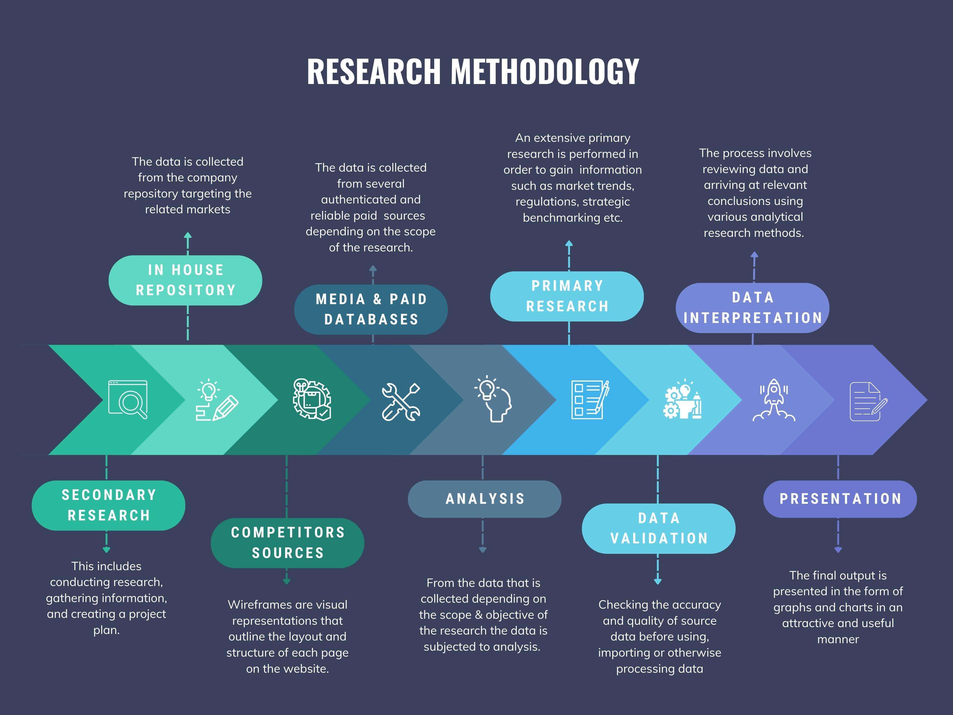
We at ‘Stratistics’ opt for an extensive research approach which involves data mining, data validation, and data analysis. The various research sources include in-house repository, secondary research, competitor’s sources, social media research, client internal data, and primary research.
Our team of analysts prefers the most reliable and authenticated data sources in order to perform the comprehensive literature search. With access to most of the authenticated data bases our team highly considers the best mix of information through various sources to obtain extensive and accurate analysis.
Each report takes an average time of a month and a team of 4 industry analysts. The time may vary depending on the scope and data availability of the desired market report. The various parameters used in the market assessment are standardized in order to enhance the data accuracy.
Data Mining
The data is collected from several authenticated, reliable, paid and unpaid sources and is filtered depending on the scope & objective of the research. Our reports repository acts as an added advantage in this procedure. Data gathering from the raw material suppliers, distributors and the manufacturers is performed on a regular basis, this helps in the comprehensive understanding of the products value chain. Apart from the above mentioned sources the data is also collected from the industry consultants to ensure the objective of the study is in the right direction.
Market trends such as technological advancements, regulatory affairs, market dynamics (Drivers, Restraints, Opportunities and Challenges) are obtained from scientific journals, market related national & international associations and organizations.
Data Analysis
From the data that is collected depending on the scope & objective of the research the data is subjected for the analysis. The critical steps that we follow for the data analysis include:
- Product Lifecycle Analysis
- Competitor analysis
- Risk analysis
- Porters Analysis
- PESTEL Analysis
- SWOT Analysis
The data engineering is performed by the core industry experts considering both the Marketing Mix Modeling and the Demand Forecasting. The marketing mix modeling makes use of multiple-regression techniques to predict the optimal mix of marketing variables. Regression factor is based on a number of variables and how they relate to an outcome such as sales or profits.
Data Validation
The data validation is performed by the exhaustive primary research from the expert interviews. This includes telephonic interviews, focus groups, face to face interviews, and questionnaires to validate our research from all aspects. The industry experts we approach come from the leading firms, involved in the supply chain ranging from the suppliers, distributors to the manufacturers and consumers so as to ensure an unbiased analysis.
We are in touch with more than 15,000 industry experts with the right mix of consultants, CEO's, presidents, vice presidents, managers, experts from both supply side and demand side, executives and so on.
The data validation involves the primary research from the industry experts belonging to:
- Leading Companies
- Suppliers & Distributors
- Manufacturers
- Consumers
- Industry/Strategic Consultants
Apart from the data validation the primary research also helps in performing the fill gap research, i.e. providing solutions for the unmet needs of the research which helps in enhancing the reports quality.
For more details about research methodology, kindly write to us at info@strategymrc.com
Frequently Asked Questions
In case of any queries regarding this report, you can contact the customer service by filing the “Inquiry Before Buy” form available on the right hand side. You may also contact us through email: info@strategymrc.com or phone: +1-301-202-5929
Yes, the samples are available for all the published reports. You can request them by filling the “Request Sample” option available in this page.
Yes, you can request a sample with your specific requirements. All the customized samples will be provided as per the requirement with the real data masked.
All our reports are available in Digital PDF format. In case if you require them in any other formats, such as PPT, Excel etc you can submit a request through “Inquiry Before Buy” form available on the right hand side. You may also contact us through email: info@strategymrc.com or phone: +1-301-202-5929
We offer a free 15% customization with every purchase. This requirement can be fulfilled for both pre and post sale. You may send your customization requirements through email at info@strategymrc.com or call us on +1-301-202-5929.
We have 3 different licensing options available in electronic format.
- Single User Licence: Allows one person, typically the buyer, to have access to the ordered product. The ordered product cannot be distributed to anyone else.
- 2-5 User Licence: Allows the ordered product to be shared among a maximum of 5 people within your organisation.
- Corporate License: Allows the product to be shared among all employees of your organisation regardless of their geographical location.
All our reports are typically be emailed to you as an attachment.
To order any available report you need to register on our website. The payment can be made either through CCAvenue or PayPal payments gateways which accept all international cards.
We extend our support to 6 months post sale. A post sale customization is also provided to cover your unmet needs in the report.
Request Customization
We offer complimentary customization of up to 15% with every purchase. To share your customization requirements, feel free to email us at info@strategymrc.com or call us on +1-301-202-5929. .
Please Note: Customization within the 15% threshold is entirely free of charge. If your request exceeds this limit, we will conduct a feasibility assessment. Following that, a detailed quote and timeline will be provided.
WHY CHOOSE US ?

Assured Quality
Best in class reports with high standard of research integrity

24X7 Research Support
Continuous support to ensure the best customer experience.

Free Customization
Adding more values to your product of interest.

Safe & Secure Access
Providing a secured environment for all online transactions.

Trusted by 600+ Brands
Serving the most reputed brands across the world.